
How to Draw a Circuit Diagram: 4 Rules for Better PCB Schematics
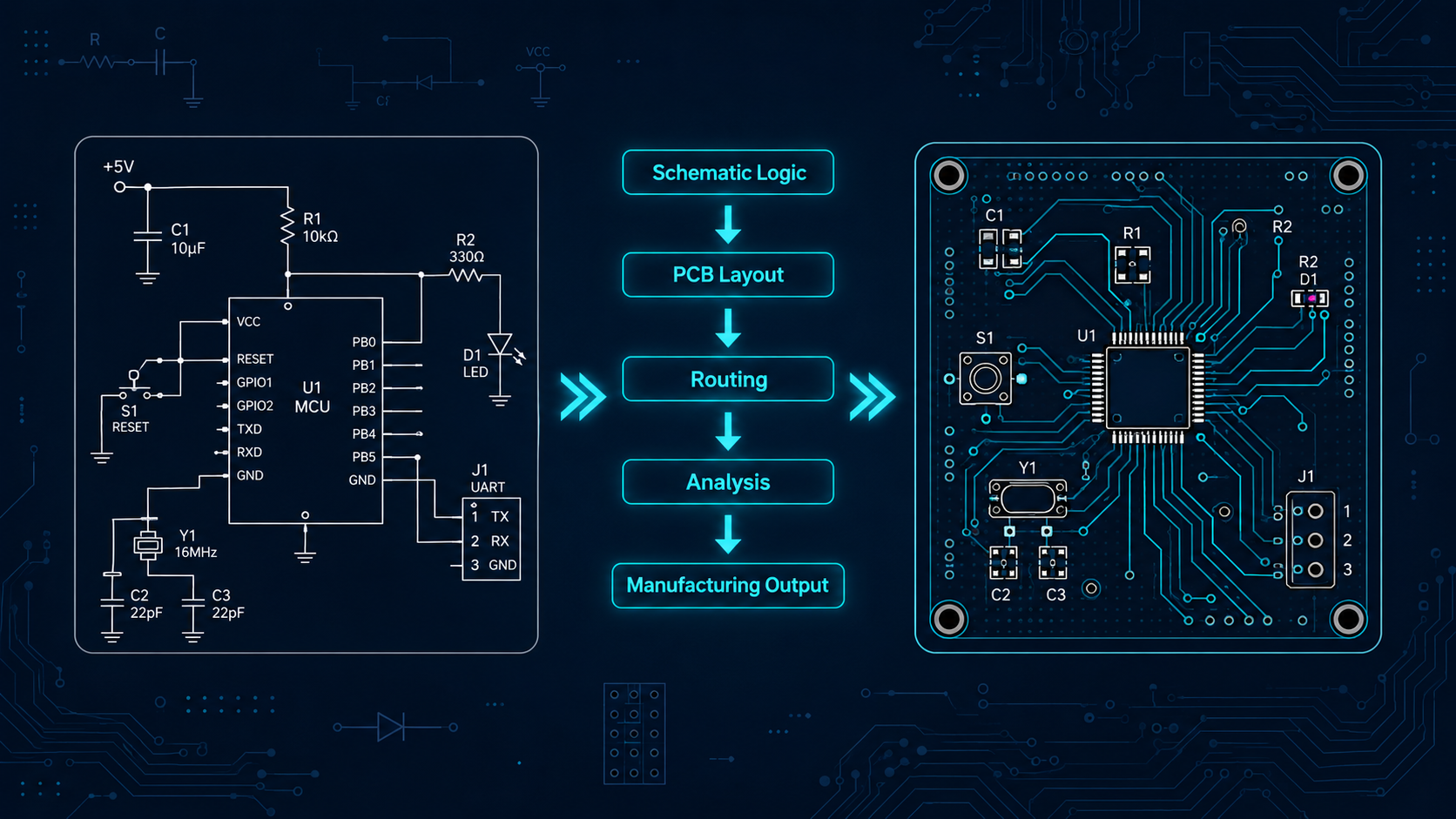
Circuit diagrams and schematics are one of the most important communication tools in electrical and electronics design. In many cases, circuit diagrams and schematics are interchangeable. For PCB teams, the schematic is the logical foundation of the board, containing implementation information such as part numbers and constraints. Before placement, routing, simulation, design review, or manufacturing output, the schematic defines the circuit’s components, connections, signals, voltage domains, and design intent.
Circuit diagrams can be logic-based without the intent of implementation. They can be used for simulation and design testing purposes. For instance, a circuit diagram may contain a generic resistor for simulation purposes. A schematic may start as a circuit diagram and evolve into an implementable schematic.
But drawing circuit diagrams or schematics is not just about placing symbols on a page. A good schematic diagram must be readable, accurate, and easy for others to follow. That includes engineers, technicians, manufacturing teams, suppliers, test engineers, and service teams.
When diagrams are unclear, small mistakes can create big problems. An unlabeled component, poor organization, or a confusing net name can lead to layout errors, rework, and delays. Those issues often surface late, when they cost more to fix.
The good news is that a few practical rules can make circuit drawing much easier. This guide explains how to draw a circuit diagram using standard conventions, a step-by-step process, and tools that help reduce errors.
For PCB design teams, the goal is not just a clean drawing. The goal is a schematic that supports layout, constraints, analysis, design review, and manufacturing.
Quick Answer: How Do You Draw a Circuit Diagram?
To draw a circuit diagram, start by defining the circuit requirements, listing the components, placing the main current path, adding branches and controls, labeling every component and signal, and reviewing all connections.
For PCB design, also confirm part numbers, net names, voltage domains, connector pinouts, test points, and design constraints before moving into layout.
What Is a Circuit Diagram?
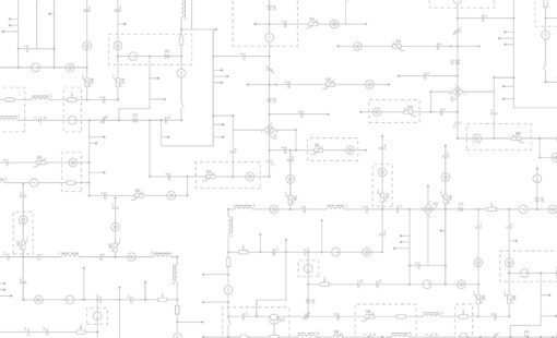
A circuit diagram is a visual representation of an electrical circuit. It uses symbols to represent components and lines to show electrical connections.
Common circuit components include:
- Power sources, such as batteries or DC supplies
- Conductors, shown as lines that connect components
- Resistors, often labeled with “R” and a resistance value
- Capacitors, often labeled with “C” and a capacitance value
- Diodes, including LEDs and Zener diodes
- Transistors, switches, connectors, and integrated circuits
- Ground or return paths, which complete the circuit
Circuit diagrams are used during design to create the logic for simulation and testing. They help teams understand electrical intent before it becomes a physical product. In many cases, the terms “circuit diagram” and “schematic” are interchangeable.
A schematic focuses on the logical electrical function of a printed circuit board (PCB) to build a PCB. A schematic contains part numbers and physical constraints for PCB layout. PCB layout translates the schematic into physical placement, routing, layers, vias, clearances, and manufacturing data. A circuit diagram may not include decoupling capacitors, whereas a PCB schematic would.
A wiring diagram is different from a schematic or circuit diagram and is used for wire harness or control panel design. It describes the physical wiring detail, such as wire routing, connectors, colors, gauges, and installation information. Wiring diagrams are not covered in this blog.
Why Schematics Matter in PCB Design
In PCB design, the schematic does more than communicate how a circuit works. It drives the downstream design process.
A well-structured schematic helps PCB teams:
- Transfer design intent into layout with fewer errors
- Map symbols to the correct footprints and component data
- Identify voltage domains, power rails, grounds, and signal groups
- Define important nets before routing begins
- Support electrical rule checks, layout constraints, and design reviews
- Create cleaner bills of materials and manufacturing documentation
Poor schematic discipline creates friction. A vague net label, a missing no-connect marker, or an inconsistent reference designator may seem small during schematic capture. Later, it can affect layout, procurement, testing, or board bring-up.
How to Draw a Schematic Step by Step
Before applying detailed drawing rules, start with a simple workflow. This helps you move from an idea or a real circuit to a readable schematic.
1. Identify the Circuit Requirements
Start by defining what the circuit must do. Is it powering a light bulb, controlling a motor, sensing voltage, or processing a signal? Identify the power source, load, control elements, protection devices, and operating conditions.
For a basic LED circuit, for example, you need a battery, a resistor, an LED, a switch, and a return path.
For PCB design, you may also define power input, voltage regulation, communication interfaces, processor connections, memory, sensors, connectors, test points, and protection circuitry.
2. List the Components
Create a component list before drawing. Include each part’s value, rating, and, if available, its reference designator. For example:
- B1: 9V battery
- R1: 330-ohm resistor
- D1: LED
- S1: switch
This step reduces missing parts and makes labeling easier later.
For PCB designs, the component list should also be connected to footprints, manufacturer part numbers, tolerances, lifecycle status, and bill-of-materials data.
3. Determine a Layout Organization
The goal is to select a layout that is easy to read and aligns with the design intent. For simple 1-page schematics, the design flow usually moves from left to right. Power is usually on top, with ground on the bottom.
For large multi-page schematics, organization is related to common functions. The CPU complex, along with memory, power monitoring, and related components, is on the same page. There may be another page that contains communication or control functions. Organization by function is a common approach.
Hierarchical design is another option for large, complex schematics. Functions are represented by blocks. A top-level schematic page contains the blocks with connections. The detailed schematic lies under the block. Not all schematic entry systems support hierarchical design.
4. Add Branches, Controls, and Supporting Components
After the main path is clear, add branches, sensors, connectors, protection devices, and control logic. Try to keep components within a function grouped together. This will consolidate related symbols into a single sheet or into a single area on a sheet.
For PCB designs, this is also where you add decoupling capacitors, pull-up and pull-down resistors, test points, programming headers, optional circuitry, and variant-specific components.
5. Label Everything Clearly
Add reference designators, values, wire names, voltage labels, and connector pin numbers. Clear labels help readers understand the circuit without having to guess.
For PCB workflows, labels also support footprint assignment, BOM generation, simulation setup, layout constraints, and manufacturing review.
6. Review the Diagram
Many schematic entry systems have design rule checking (DRC). DRC’s can be used to check a variety of potential entry errors. Some examples include unconnected components, pins, connections missing a source or load, and missing reference designators. Some DRC checks can go to the next level and perform electrical checks on source and loading characteristics.
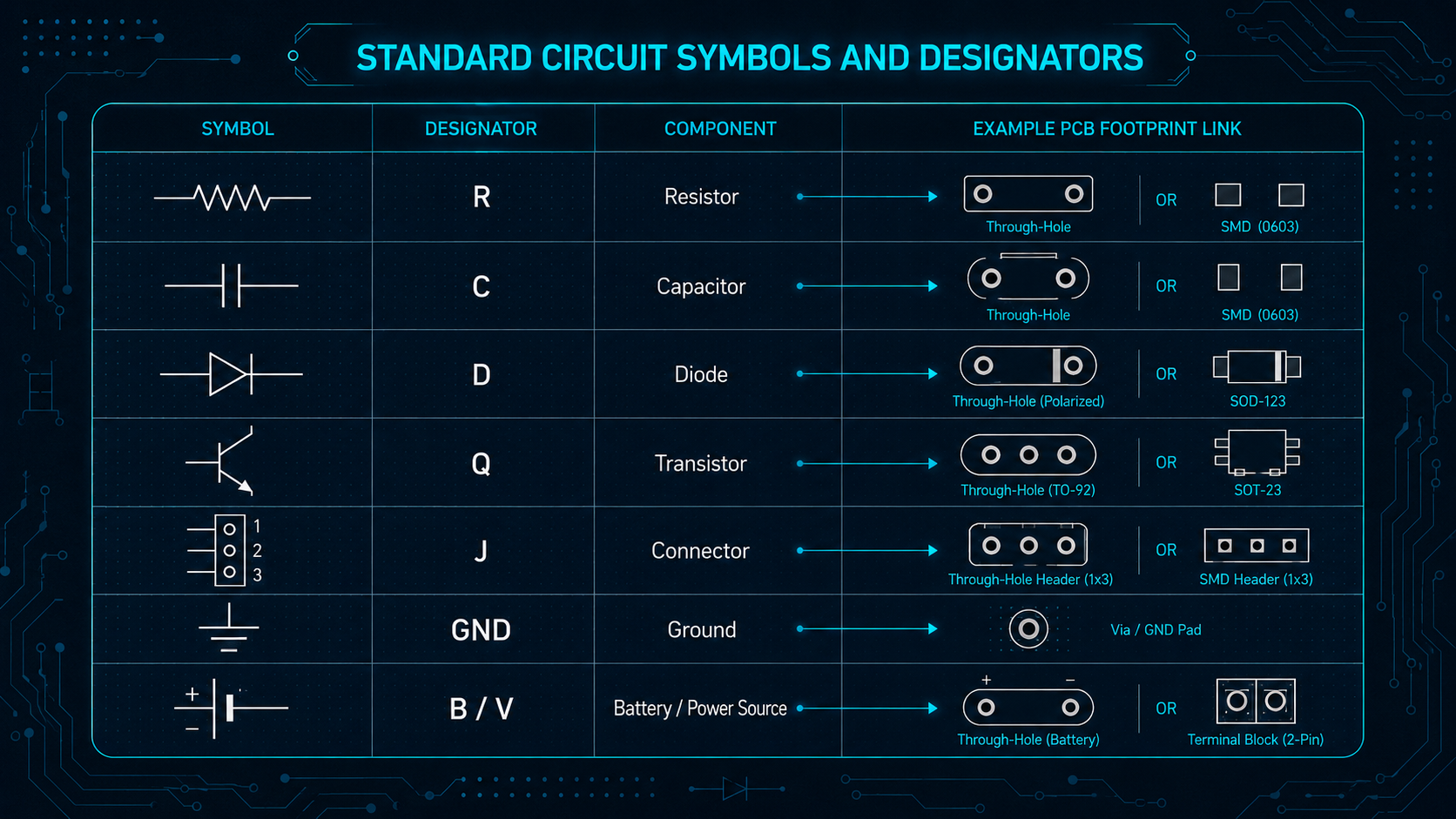
Rule 1: Use Standard Circuit Symbols
A schematic entry system will usually come with a starter library, or you can connect to a shared corporate library. Either way, the symbol can be a logical system (i.e., an AND gate) or a component (i.e., an FPGA).
Generic symbols would include resistors, capacitors, inductors, batteries, switches, diodes, transistors, and connectors. Using these symbols consistently helps engineers and technicians understand the design without needing extra explanation.
Reference designators also matter. A resistor is typically labeled “R,” a capacitor “C,” a diode “D,” a transistor “Q,” and a connector “J” or “P.” These labels make it easier to cross-reference the schematic with a bill of materials, PCB layout, wiring diagram, or test procedure.
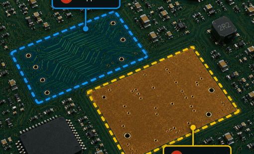
For PCB teams, the symbols are just part of the component. The component is typically uniquely identified by the part number. The schematic symbol is mapped to a footprint used to lay out the board. Pin 1 on the symbol maps to pin 1 on the footprint. When symbols and footprints fall out of sync, the risk of schematic-to-layout errors increases.
For professional engineering teams, a controlled component library is important. It keeps symbols, part data, and naming rules consistent across projects.
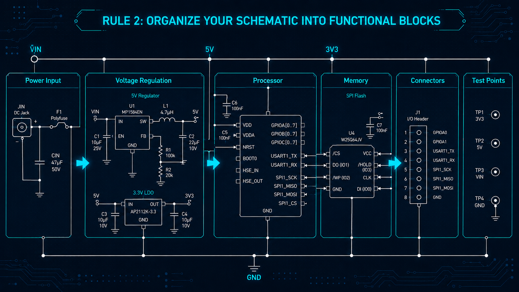
Rule 2: Keep the Layout Logical and Consistent
A readable schematic should guide the eye through the circuit. Place components in a logical order so the reader can trace the function without jumping around the page.
In many schematics, signals flow from left to right. Power often appears at the top, with ground or return paths near the bottom. This is not a strict rule for every design, but consistency matters.
Avoid unnecessary wire crossings. Keep component orientation consistent where possible. Group related circuit sections, such as power regulation, input conditioning, switching, and output control.
For PCB designs, group the schematics by functional blocks. Common sections include power input, voltage regulation, processor or FPGA circuitry, memory, analog front end, communication interfaces, connectors, and test/debug circuitry.
This organization helps reviewers evaluate the design before layout begins. It also makes it easier to spot missing pull-ups, unclear power rails, inconsistent connector pinouts, or weak test coverage.
For larger electrical systems, use hierarchical blocks, sheet references, and net labels. These tools help readers follow signals across multiple pages without losing context.
Good layout reduces cognitive load. That is especially important when diagrams support design reviews, supplier communication, manufacturing, or service documentation.
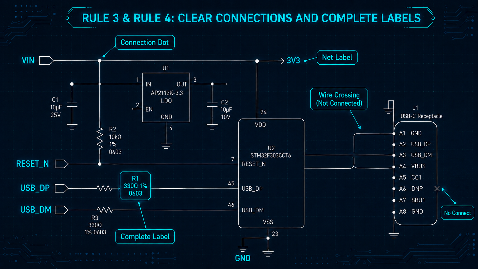
Rule 3: Make Connections Unambiguous
Connection clarity is one of the most important parts of circuit drawing. A single unclear crossing can change how someone interprets the circuit.
Use net labels for important signals, such as VIN, GND, 5V, CAN_H, CAN_L, or RESET. Net labels are especially helpful when a connection continues on another sheet.
For PCB teams, net naming matters because layout depends on signal identity. Clear names help designers identify differential pairs, voltage domains, clock signals, reset lines, controlled-impedance routes, and ground strategy before layout begins.
Examples include USB_DP, USB_DM, ETH_TX_P, ETH_TX_N, 3V3, 5V, VBAT, RESET_N, CLK_25M, AGND, DGND, and CHASSIS_GND.
Also, clearly mark no-connect pins. This indicates that an unused pin was intentionally left open. Without this marking, reviewers may wonder whether the omission is a mistake.
Rule 4: Label Components, Values, and Signals Clearly
Every component should have a clear label. At a minimum, include a reference designator and value. For production designs, include part numbers, tolerances, ratings, and connector pin information where needed. This information is typically in the component library and applied automatically.
Labels also support troubleshooting. If a technician measures the voltage at TP1, checks R4, or verifies pin 7 on J2, the diagram must make those locations easy to find.
In PCB workflows, labels also support BOM generation, footprint assignment, variant management, simulation, board bring-up, and manufacturing review. Reference designators, values, tolerances, voltage ratings, package information, and test-point labels all help reduce ambiguity.
Good labeling also supports automation. In professional electrical design software, reference designators, part data, wire names, and reports can be connected. That helps generate bills of materials, wire lists, from-to tables, and manufacturing documentation with fewer manual errors.
How Zuken Supports PCB Schematic and Circuit Design
Zuken CR-8000 helps PCB teams move from schematic intent to layout, constraints, analysis, and manufacturing outputs. Instead of treating the circuit diagram as a static drawing, CR-8000 connects schematic data with the downstream design process.
CR-8000’s Design Gateway schematic entry tool supports the logical circuit design and verification of single- and multi-board electronic systems. It helps teams manage signal continuity, including board-to-board interconnects, at the system level.
CR-8000 also supports architecture design and verification, multi-board PCB layout with MCAD integration, signal and power integrity analysis, and chip/package/board co-design for complex PCB subsystem designs.
For PCB teams, this matters because schematic decisions influence layout, constraints, analysis, procurement, and manufacturing. Zuken’s constraint-driven methodology also supports consistency across schematic capture, PCB layout, and SI analysis.
E3.series supports electrical wiring, control systems, harness design, and panel documentation. It helps teams create intelligent diagrams connected to parts, wires, connectors, and downstream manufacturing data. This supports clearer schematics, stronger wiring documentation, and fewer manual handoff errors.
For engineering leaders, the benefit is bigger than drawing speed. Governed circuit diagram design improves communication, supports audit-ready documentation, and helps teams protect quality as complexity increases.
Conclusion: Better Schematics Reduce PCB Design Risk
Learning how to draw a circuit diagram starts with the basics: standard symbols, logical layout, clear connections, and complete labels. These rules help anyone create diagrams that are easier to read, build, review, and troubleshoot.
For PCB teams, those same rules also support cleaner schematic-to-layout transfer, stronger design reviews, better constraint management, and fewer late-stage corrections.
For simple projects, free circuit diagram tools may be enough. For professional engineering teams, intelligent design platforms provide the consistency, validation, and digital continuity needed to manage complexity.
As electrical systems become more connected and documentation demands increase, clear circuit diagrams are more than drawings. They are a foundation for better collaboration, faster reviews, and more reliable products.
Next step: Explore how Zuken’s CR-8000 helps PCB teams connect schematic design, constraints, layout, analysis, MCAD integration, and manufacturing outputs into a single integrated design flow.

-
Vice President of Marketing, Zuken USA, Inc.


- Blog

- Blog
- Blog

- Blog
Related Products and Resources
- Blog

- Blog

- Products
E3.series is a Windows-based, scalable, easy-to-learn system for the design of wiring and control systems, hydraulics and pneumatics. The out-of-the-box solution includes schematic (for circuit and fluid diagrams), cable (for advanced electrical and fluid design), panel (for cabinet and panel layout), and formboard (for 1:1 wiring harness manufacturing drawings). Integrated with MCAD, E3.series is a complete design engineering solution from concept through physical realization and manufacturing output.

- Products
Building a competitive product today is much more difficult than a few years ago. Existing PCB-centric design processes are limited to a single PCB and do not provide the necessary tools for today’s competitive product development environment. PCB-centric design processes are falling behind.