
Tech Tip: Template Area Net Check Prevents Copper Net Mismatches
Complex PCBs change quickly as projects mature. This ongoing change can introduce design errors that lead to costly rework and delays. The Template Area Net Check in Design Force helps teams stay aligned through every revision by catching copper fill net mismatches between schematics and PCB design before they become problems.
Why Copper Fill Area Net Accuracy Matters
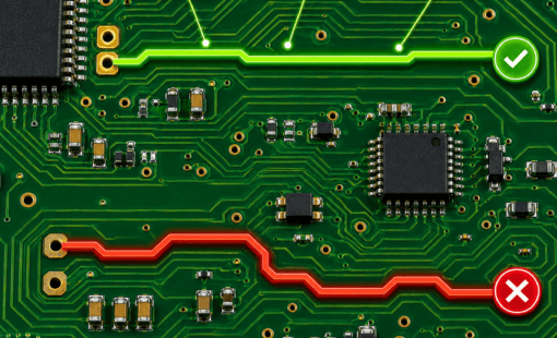
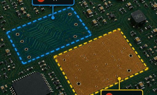
Copper fills are large conductive areas added to a PCB to carry power, improve grounding, or reduce noise. They must be accurately assigned to the correct nets so they function as intended in the schematic. When a copper area is tied to the wrong net, it can float and disrupt power or signal integrity.
Aligning PCB Schematic and Design Teams
Schematic and layout teams often move quickly, and even small changes can cause net mismatches between the logical design and the physical board. Ensuring every copper area reflects the latest schematic update keeps the layout stable and prevents errors from slipping downstream. A clear verification step helps both teams stay aligned through frequent revisions.
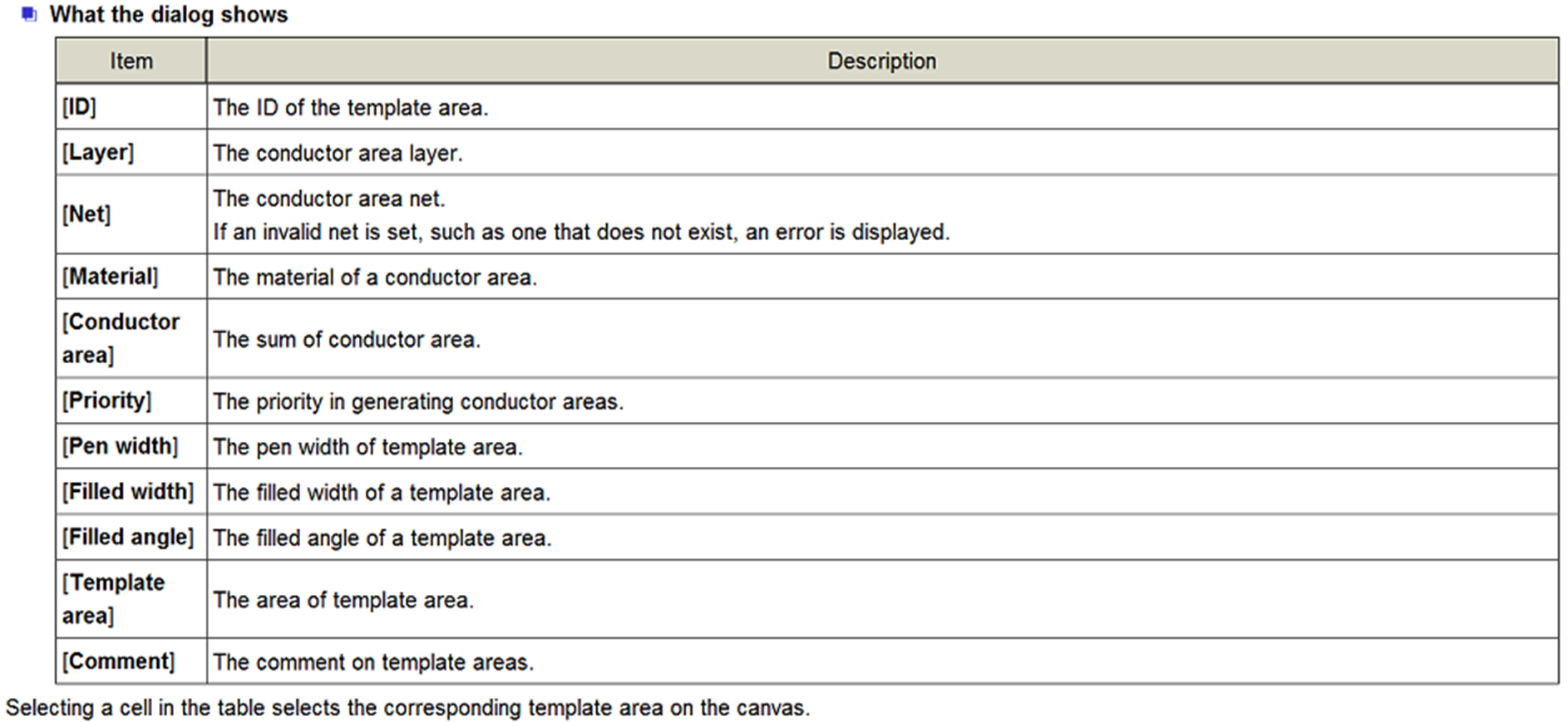
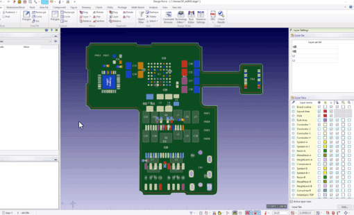
What is the Template Area List?
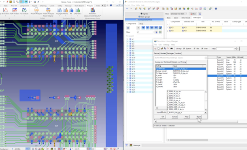
The Template Area List in CR‑8000 Design Force is a centralized view of all template areas in a layout. It shows key details like assigned net names, fill type, and generation status in a clear, sortable table.
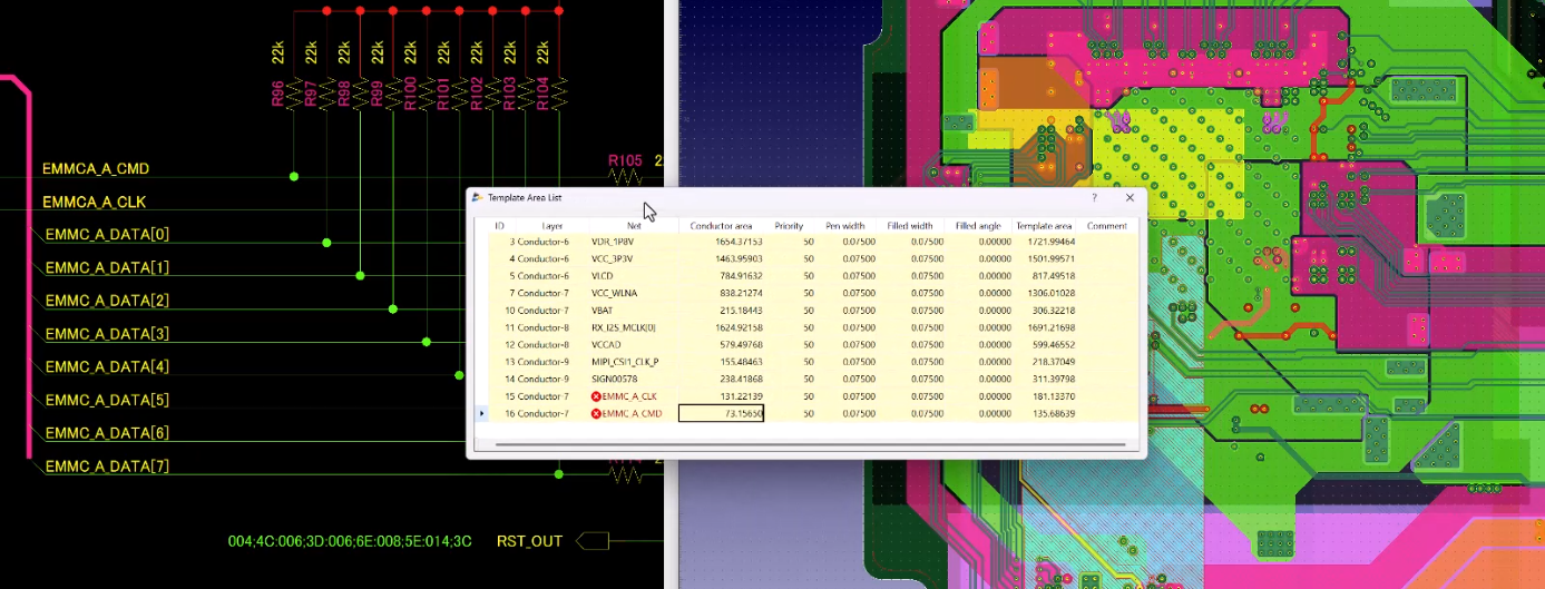
With this feature, engineers quickly verify that copper fills and mesh planes are tied to the correct nets. This visibility helps catch mismatches early, streamline reviews, and reduce the risk of floating copper in complex, reuse-heavy projects.
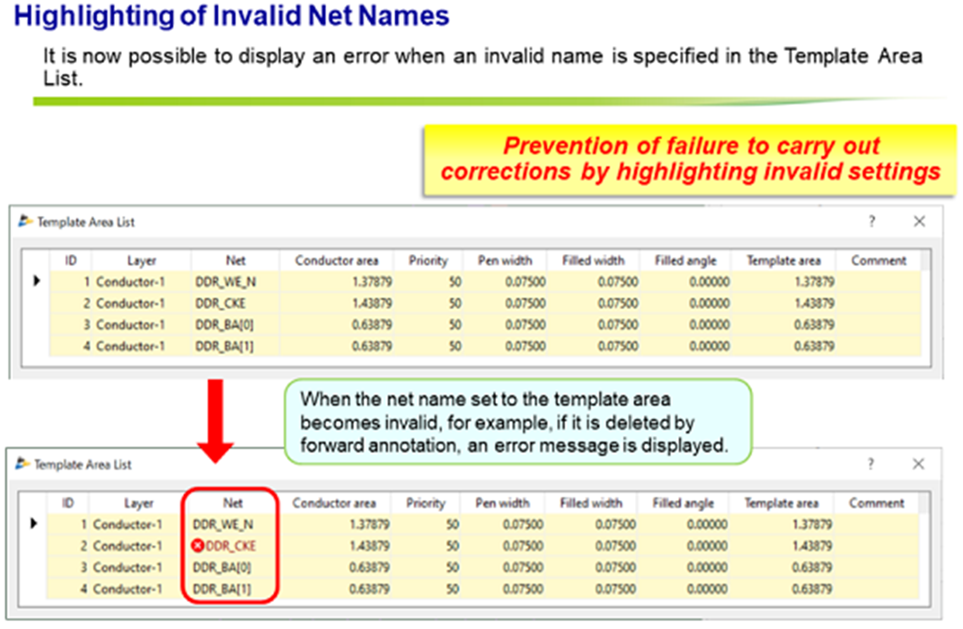
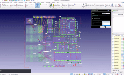
How Template Area Net Check Works in CR-8000 Design Force
- CR-8000 cross-references signal names in the Design Gateway schematic with template areas in the Design Force layout
- The system flags invalid template areas that are assigned nets that don’t match the schematic
- The Template Area List table clearly displays the results
This helps engineers easily spot invalid nets and quickly reassign nets to areas, keeping the PCB layout aligned with the latest schematic.
To access the Template Area List, click the following on the ribbon: [Area Fill] – [Template Area] – [Template Area List].
Who Benefits from Template Area Net Check?
- PCB Layout Engineers
- Why it helps: Flags invalid net names early, preventing floating copper fills and mesh planes.
- Benefit: Reuse templates with confidence and avoid costly redesigns by accelerating layout verification
- DFM and Manufacturing Teams
- Why it helps: Ensures copper areas are correctly tied to nets before fabrication
- Benefit: Reduces risk of yield loss and manufacturing defects caused by unconnected copper
See Template Area Net Check in Action
Next Steps: Strengthen Your Electronic Design with CR-8000
The Template Area Net Check is part of a broader analysis toolbox in CR-8000 that helps teams design faster with fewer errors. Combined with power integrity, signal integrity, and system-level analysis, it ensures revisions don’t compromise the final design.
To learn more about how Design Force supports advanced PCB and IC package design, visit the CR-8000 Design Force product page or explore related articles such as System-Level PCB Analysis: Managing Complexity in Electronic Systems.

-
Applications Engineer

- Blog
- Blog

- Blog

- Blog
Related Products and Resources
- Blog
- Blog
- Blog
- Products
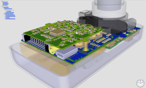
Design Force combines traditional 2D design with native 3D design and the latest human interface techniques, accelerated graphics and almost instantaneous rendering and refreshing. It is the fastest, most effective PCB design solution available today. Design Force enables design teams to layout their designs in the context of a complete system or product.