
Tech Tip: Check PCB Trace Resistance with Ohmic Distance in CR-8000
Printed Circuit Board (PCB) traces are not perfect conductors. As current moves through a routed copper path, PCB trace resistance is affected by the trace’s length, copper thickness, and temperature. In critical circuits, excessive resistance harms performance through voltage drops, signal integrity issues, and measurement errors.
CR-8000 Design Force helps designers evaluate these risks with the Ohmic Distance tool. Designers can measure resistance directly on the PCB layout or define resistance limits for multiple pin pairs to check critical connections during design updates.
PCB Layout is Part of Circuit Performance
PCB design is not complete when every component is connected. The physical layout of each route can influence how the circuit behaves in the real world. For critical connections, designers need to confirm that the routed path supports the design’s electrical intent.
Why PCB Trace Resistance Matters
Trace resistance is the electrical resistance along a copper path on a PCB. Every trace has some resistance, although the value is often small. For critical circuits, too much resistance can affect voltage delivery, heat generation, signal quality, and measurement accuracy.
The trace resistance equation is as follows:
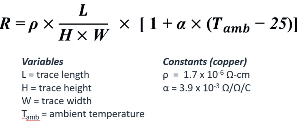
In simple terms, resistance increases when the trace gets longer, narrower, thinner, or hotter.
If trace resistance is too high, it can create several power distribution issues:
-
Voltage drop
Small resistance values can cause meaningful voltage loss when the current is high. For example, a 10 mΩ trace carrying 5 A creates a 50 mV drop, which can be significant for low-voltage rails with limited operating margin. -
Power delivery instability
Devices with tight supply requirements need voltage to stay within a narrow range. Excess trace resistance can reduce the voltage delivered to the load and make the circuit more sensitive to current changes. -
Thermal stress
Power dissipation is calculated as P = I²R. High current through excessive trace resistance can generate localized heat, contributing to copper degradation, solder joint stress, and long-term reliability risks.
Excess trace resistance can also lead to signal integrity issues, including:
-
Signal loss
Excess trace resistance can attenuate signals as they travel across the board. Signal loss is especially important for high-speed digital buses, RF paths, and other circuits where signal strength affects reliable operation. -
Controlled impedance
Some high-frequency PCB signals require the trace to maintain a consistent controlled impedance. Excess trace resistance can change the impedance characteristics of the transmission line, causing reflections that superimpose on the primary signal and create distortion. -
Measurement and control errors
In sense lines or feedback loops, trace resistance can add unintended series resistance. This additional resistance can affect measured values and contribute to regulation drift.
How CR-8000’s Ohmic Distance Tool Calculates Trace Resistance
CR-8000 Design Force contains the layout data needed to evaluate PCB trace resistance, including the routed path, cross-sectional area, and copper properties. The Ohmic Distance tool uses this data to calculate resistance directly between two selected points on the canvas.
Designers can also select the trace temperature before running the calculation. Selecting the trace temperature matters because copper resistance increases as temperature rises. Temperature-aware analysis helps the result better reflect real operating conditions.
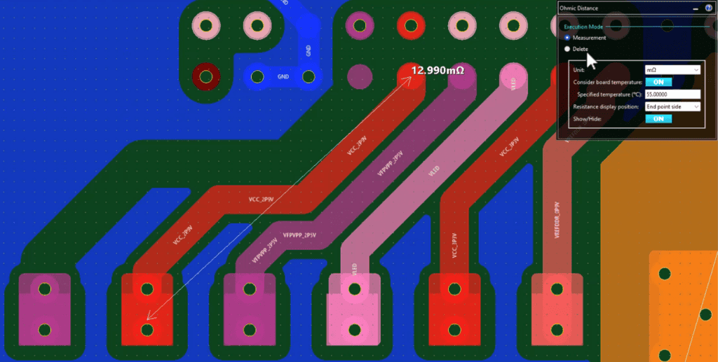
Instead of estimating resistance outside the PCB design environment, designers can utilize CR-8000 to calculate resistance from the actual routed copper path.
Benefit: Immediate visibility into potential problem areas without needing external calculations.
See Ohmic Distance in Action
How to Check Multiple Trace Resistance Limits at Once
Ohmic Distance can also be used through the Constraint Browser for a more systematic design check. Designers define pin pairs for critical connections and the minimum and maximum trace resistance allowed for each pair. The table automatically evaluates compliance during design updates.
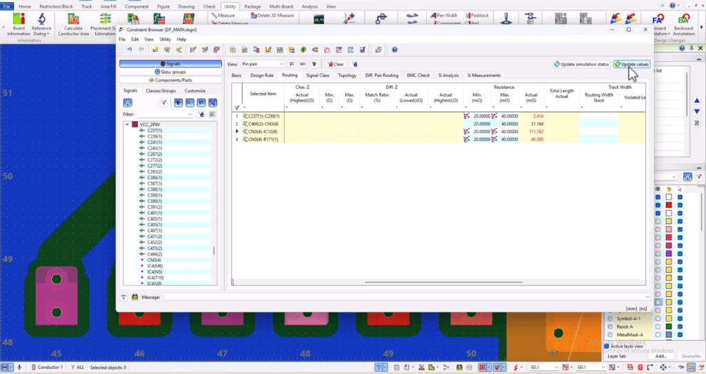
Teams can move from one-by-one manual checks to constraint-driven validation. Resistance violations are clearly flagged (e.g., highlighted in red) in the constraint system. Clear violation markers enable rapid identification and correction of power delivery weaknesses and signal integrity risks.
By integrating Ohmic Distance analysis and resistance constraints into the design workflow, CR-8000 Design Force enables:
- Proactive issue prevention instead of reactive debugging
- Faster design iterations with built-in validation
- Improved product reliability and performance
- Reduced risk of costly redesigns or field failures
Benefit: Resistance targets are enforced systematically, not dependent on manual checks.
Who Uses Ohmic Distance
PCB Layout Designers
PCB layout designers use Ohmic Distance to measure trace resistance directly on the board layout. Direct measurement helps them adjust trace width, routing length, copper usage, or layer choices before the design moves further downstream.
Electrical Engineers
Electrical engineers use Ohmic Distance to confirm that critical circuits meet performance expectations. Ohmic Distance is especially useful for power rails, high-current connections, precision measurement circuits, and other nets where resistance can affect circuit behavior.
Design Review Teams
Design review teams use resistance constraints to verify that important pin pairs meet defined limits. Constraint-based verification creates a more consistent approval process and helps teams identify potential issues before fabrication.
Next Steps: Strengthen Your PCB Design with CR-8000
PCB trace resistance is easy to overlook, but it can affect voltage drop, heat, signal quality, measurement accuracy, and long-term reliability. CR-8000 Design Force helps designers check resistance directly from the PCB layout and apply resistance limits to critical pin pairs through the Constraint Browser.
Adding trace resistance checks to the design workflow, teams can find issues earlier and improve confidence before board approval.
To learn more about PCB design with CR-8000:
- Visit the CR-8000 product page
- Read more PCB layout validation tech tips
- Watch this webinar on signal and power integrity in high-speed designs

-
Applications Engineer

- Blog

- Blog
- Blog

- Blog
Related Products and Resources
- Blog

- Blog
- Blog
- Blog