Tech Tip: Using Inhibit Layers to Clear Trace Patterns
Menu
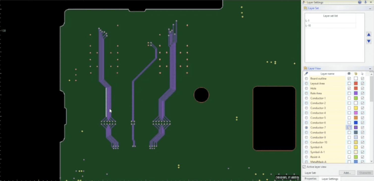
In this tech tip, we will explore how you can clear a routed trace pattern on multiple conductive layers.
In this design, the requirement is to have these traces on layer 7 to be cleared in the exact same pattern on the conductive areas which are poured on layers 6, 7 and 8.
In this completed example you will see we have these traces routed and they have been cleared on the plane on layer 7. Also, take note that the routed traces have clearances defined on layers 6 and 8.
During today’s tech tip I am going to show you how it’s done!
What we will need is an only track keepout inhibit layer defined that are associated with layers 6 and 8. To set this up I will launch the technology editor. First I will create a user-defined layer and call it InhibitTrack_Layers_6_8. Next, I will right click over the new user-defined layer and select associate with the conductive layer. In this next dialog, I will select both layers 6 and 8 and then set the Layer Type to “Only track keepout” and then select Association. Now take note that this layer is associated with layers 6 and 8.
Next, I will set the active layer to InhibitTrack_Layers_6_8 and I will select the Figure tab and select Offset.
Now I will use the Offset function located on the Figure tab of the ribbon.
In the parameters, dialog set the “Mode” to Area Fill and then set the direction to Outside. Then set the offset value to .1. Next, I will frame select the traces and the offset is generated on to InhibitTrack_Layers_6_8
So far so good!

Sandy Jones is a Director of Customer Support ensuring customers are well taken care of by guiding her team to achieve support excellence. Her work focuses on improving customer support procedures through regular communication along with managing training activities and materials. In her free time, she enjoys repurposing old barn wood windows by painting images on the glass.
During her free time she enjoys gardening, water-color and acrylic painting and being actively involved in a women’s social/service organization.

- Blog
May 23, 2025
AI in PCB Design: From Misconception to Meaningful Assistance
AI in PCB design is increasingly seen as a game-changer, with some predicting it could soon replace entire layout teams—but this view risks overlooking both the current limits of AI and the critical expertise engineering demands. At DesignCon 2025, experts from emphasized that AI's real value lies in complementing human judgment, not replacing it. Read more on our blog.
Read now

- Blog
February 13, 2025
The Future of Augmented Reality
Our new post explores the potential of augmented reality (AR) to transform everyday experiences in shopping, education, and navigation. It highlights how enhanced AR devices will offer immersive, interactive environments that blend the virtual and physical worlds.
Read now

- Blog
January 30, 2025
The Top PCB Design Trends to Watch in 2025
The field of PCB design continues to evolve as advancements in technology and shifting market demands push the boundaries of what’s possible. By 2025, several key trends are set to shape the industry. Find out more on our blog.
Read now

- Blog
January 23, 2025
Supply Chain Risk Management in PCB Design with SiliconExpert and CR-8000 Integration
Supply chain risk management is critical for electronics design. By integrating SiliconExpert with CR-8000, engineers gain tools to streamline component selection, manage obsolescence, and ensure design continuity. This integration supports efficient workflows, reduces costs, and mitigates supply chain disruptions.
Read now
