

Signal Integrity Unplugged: Practical Ways to Make High-Speed Links Work
Guest experts: Donald Telian (SI Guys) and Ralf Brüning (Zuken)
Menu
High-Speed Links and the SI Fundamentals Revisited
The design of High-speed serial link often leaves design engineers feeling that the days of “Signal Integrity equals Black Magic” have returned as data rates climb relentlessly. A recent SI Guys conversation between Donald Telian and Ralf Brüning brings it back to first principles. Learn the important principles, and SI becomes and understandable engineering discipline.

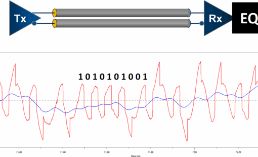
For those of you not being in touch with High-Speed Links and SerDes on a daily basis, Serializer/Deserializer (SerDes) defines a data transmission technology used in modern high-speed communications to overcome the limits of former data transmission methods. The primary use of a SerDes is to provide data transmission over a single line or a differential pair in order to minimize the number of I/O pins and interconnects. SerDes links are the primary solution used in all the highest-speed interfaces, such as PCIe, Ethernet, SATA, HDMI, Display-Port, Fast USB and many more.
The good news is that, electrically, all serial links are the same.
In practical terms and from high-level, reliable links come down to understanding and taming Loss and Discontinuities. For example, even short stubs can be catastrophic near the quarter-wavelength, and reflections from small structures (e.g.; vias) will create inter-symbol interference (ISI) that damages signal integrity.
As a consequence, modern receivers increasingly lean on equalization to cope with this problem. This article, Ralf and Don’s conversation, and in particular Don’s LIVE Gen2 SI Class in Munich, distils these points for electronics designers who aren’t necessarily SI specialists—and shows where the right approach help you avoid and catch problems before they hit the lab.
Watch the conversation
Signal Integrity Unplugged: An Expert-to-Expert Conversation (20 mins)
Loss vs. discontinuities: two different ways to lose a signal
Every high-speed interconnect shows some loss behaviour, hence a fraction of the transmitted energy will not arrive at the receiver. Loss is the predictable attenuation from the configuration of the copper and the dielectric; it steadily reduces the signal amplitude with frequency and transmission distance. Discontinuities—vias, pads, connectors, abrupt stackup or geometry changes—create impedance mismatches that reflect some energy back toward the source. Those reflections overlap subsequent bits and close the eye in a way equalization can’t always untangle. A good first step in any project is to decide which problem is the primary one in your link. Long backplanes or cables are often loss-constrained (focus on materials, length, and equalizer headroom). Short, modular interconnects with multiple transitions are typically reflection-limited (hunt down and tame the mismatches first). Budgeting with a bit of skilled detective work is key for success here!
Why stubs are the “bugaboo” (especially near quarter-wavelength)
A stub is any unterminated spur off your main path—a branch trace, the unused part of a via barrel, a lingering test pad. At low frequencies their effect can often been ignored while at high frequencies it can squelch your signal. When a stub length approaches λ/4 (quarter of the wavelength) at energy-bearing frequencies, the reflection returning from the open end is nearly 180° out of phase and can cancel the high-frequency signal on your main path. Practically, that means the eye height collapses even though the physical stub looks physically “short.” As data rates rise, stub lengths that once didn’t matter suddenly do, and Telian’s popular “SI Cheat Sheet” helps you understand what matters when. The fix is straightforward but non-negotiable: remove or shorten stubs (e.g., backdrill unused via barrels, choose layer pairs that minimize via length, avoid stray branches and test pads on high-speed nets). Treat stubs as high-risk items in design reviews.
Reflections, ISI, and the importance of impedance consistency
Reflections don’t just shave amplitude; they smear time. Echoes show up as extra bumps after a transition, bleeding into the next unit intervals—that’s ISI. The closer a discontinuity sits to the transmitter or receiver, the more impact it will have. The antidote may sound boring but is very powerful: keep impedance consistent from die-pad to die-pad. Package breakout, via geometry, connector launch, trace width/height, and stackup transitions should be managed as one continuous transmission line. If you must change something (layer, medium, geometry), make the transition smooth and intentional, not abrupt and accidental. And when, for some reason, you’re stuck with the impedance of a certain feature, Telian’s articles at SI Journal provide seven more ways to handle your discontinuity.
Impedance matching: no more guesswork with modern tools
Achieving consistent impedance and minimal discontinuities might sound labor-intensive, but modern PCB tools make it practical. The right environment lets you plan trace/stackup impedance up-front and check the results while you lay out—so you catch problems before fabrication. Zuken’s CR-8000 Design Force includes an integrated EM field solver for trace/stackup impedance planning and TDR-style impedance checks during layout. When you need detailed 3D via characterization, Design Force connects to partner solvers (e.g., Ansys or Keysight) to analyze and minimize the impact of via geometries for example.
Historically, many teams sized only trace widths and overlooked the via effects. Above ~10 Gb/s, via-induced reflections become significant in standard PCBs. In-flow impedance planning combined with targeted 3D analysis lets you tune drill diameters, pads, return-path vias and anti-pads to reduce reflections where they matter most. A pragmatic workflow emerges: simulate early to decide whether your link is loss-constrained or reflection-limited, fix the physical causes (e.g., remove stubs, smooth launches, optimize stackup), and only then apply the correct equalization. Tight design-analysis loops shorten schedules and prevent expensive re-spins.
The rise of Rx Equalization—and what it’s telling you
Receivers today ship with increasingly powerful equalization, notably longer DFE (Decision Feedback Equalizer) tap chains, more CTLEs, and even FFEs. That’s a symptom of channels carrying more ISI across more unit intervals. It’s impressive silicon—but it’s not a license to ignore solid layout practices. Robust links are built in copper first and finished in silicon, not the other way around.
What this means for your day-to-day flow
On all design projects, fundamentals win. Begin designs by classifying risks as loss or discontinuities. Treat stubs as show-stoppers. Use impedance planning and TDR checks in-flow to keep the impedance consistent. Use equalization for polish, not rescue. Teams that follow this order spend less time in the lab, see faster bring-ups, and avoid “mystery” failures late in test.
Next steps and resources
- Read the previous article in this series. For complementary context, see:
- Join expert training. If you want hands-on depth with vendor-neutral best practices, attend Donald Telian’s LIVE ‘Signal Integrity, in Practice’ Gen2 SI Class near the Munich Germany Airport (October 29–30, 2025). It’s a focused way to turn these principles into repeatable lab and layout habits. Register soon at www.siguys.com/training
Explore CR-8000 for high-speed design.
- Learn how CR-8000 Design Force SI Advance supports constraint-driven layout, in-design SI checks, and 3D co-design to minimize discontinuities.
- Watch an on-demand high-speed design webinar from our Signal Integrity / Simulation Webinar Library
- Browse CR-8000 training options to get your team productive on CR-8000’s SI workflow.
- If you’re evaluating tools, request a tailored demo or trial to try your stackups, vias, and channels on a real design.
Conclusion.
As line rates climb, the path to reliable links doesn’t change: fix the copper, then finish in silicon. By tackling loss vs. discontinuities deliberately, eliminating quarter-wave stubs, enforcing impedance consistency, and using just-enough equalization, you’ll ship cleaner designs with fewer surprises. Modern, analysis-aware PCB tools—backed by focused training—make those fundamentals easier to apply, day after day.

-
Author/Signal Integrity Specialist - SIGuys.com
Donald Telian has pioneered Signal Integrity for more than 40 years. For the last 20 years he has been a Consultant, focused on designing serial links into products from flash drives to switches with thousands of links. He has invented various SI concepts, tools, and quirks engineers use everyday to get their jobs done. He is widely known as the originator of IBIS, PCI, and the author of “Signal Integrity, In Practice” – a new book and LIVE 2-day class Gen2 SI that cuts through the noise to explain how to “do” SI when confronted with the data rates of today. Learn more at siguys.com.
- Blog
August 19, 2025
High‑Speed Serial Link Design: The TWO Things That Make Links Work (and Fail)
Learn the two key fundamentals for reliable high-speed serial link design and how to overcome signal integrity challenges at multi-Gbps speeds.
Read now
Guest author: Donald Telian (SI Guys) – Signal‑integrity veteran, IBIS co‑founder, and author of Signal Integrity, In Practice.

- Blog
May 23, 2025
AI in PCB Design: From Misconception to Meaningful Assistance
AI in PCB design is increasingly seen as a game-changer, with some predicting it could soon replace entire layout teams—but this view risks overlooking both the current limits of AI and the critical expertise engineering demands. At DesignCon 2025, experts from emphasized that AI's real value lies in complementing human judgment, not replacing it. Read more on our blog.
Read now

- Blog
February 13, 2025
The Future of Augmented Reality
Our new post explores the potential of augmented reality (AR) to transform everyday experiences in shopping, education, and navigation. It highlights how enhanced AR devices will offer immersive, interactive environments that blend the virtual and physical worlds.
Read now

- Blog
January 30, 2025
The Top PCB Design Trends to Watch in 2025
The field of PCB design continues to evolve as advancements in technology and shifting market demands push the boundaries of what’s possible. By 2025, several key trends are set to shape the industry. Find out more on our blog.
Read now