
PCB constraints should drive your design flow. Here’s why.
We’ve all heard of PCB design constraints. They’re those little things that limit our ability to create the perfect board in very short periods of time. But what exactly are they? And why do they matter? This blog post elaborates on PCB constraints and why they should drive your design flow.
A modern PCB, like the one you might find inside a smartphone or laptop, is a marvel of the electronic engineering age. A circuit board takes multiple parts – metals, plastics, insulators, smart pieces of silicon, solder joints, etc. – and assembles them into something useful. But while it sounds simple enough, there are a number of factors that must be considered during the design process to ensure a reliable and manufacturable product.
One of those factors is the more and more constraint management of the PCB layout process. From a high-level perspective, PCB constraints are used for defining the physical characteristics of a PCB to prevent manufacturing problems and to ensure the electrical performance of the board as well. PCB constraints are often neglected in the design process even though they play an increasingly important role in the final product’s reliability.
Types of PCB Design Constraints
PCB constraints fall into the following categories:
- Length constraints impose restrictions on routing length for nets and net branches and include minimum length, maximum length, and matched length.
- Routing constraints impose restrictions on the length of routes and branches, as well as the minimum and maximum length of these routes.
- Signal delay-based constraints: For modern technologies such as fast double data rate (DDR) memory-based systems the two constraint types above are increasingly changing into electrical signal delay-based constraints rather than physical length numbers.
- Topology constraints restrict the routing patterns for particular nets. They are used to control the routing structure and to impose length (or delay) restrictions on net branches (pin pairs).
- Clearance constraints define a minimum distance that must be maintained between different objects on the same routing layer.
- Crosstalk rules like maximum parallel routing or the maximum separation distance specify how long traces can run parallel while violating the differential spacing value. They aim to prevent unwanted electromagnetic noise and they are not specific to any one layer
- Differential pair constraints include the trace width, the spacing between differential traces or more simple a range for the differential impedance.
Defining the constraints is a balancing act. It makes the design process more robust, but it is all too easy to over-constrain and make it impossible to complete routing and placement.
In PCB design, there was a time when ECAD tools had limited capabilities to guide the designer through the design process from schematic to manufacturing. There was a lot of manual changing and visual verification in iterations involved. This worked when designs were simple, but in today’s world of multilayer, high-density, high-speed PCB layouts, there’s just too much to look for.
Thankfully, modern ECAD tools like CR-8000 Design Force have a built-in rule- and constraint-system that holds all constraint data making the process easier and more reliable.
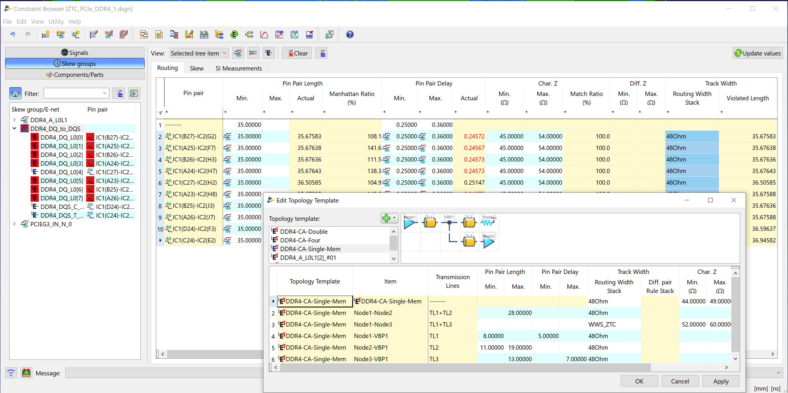
PCB Design Rules and Constraint definition in CR-8000
In CR-8000 Design Force designers can set the global parameters, such as default trace widths and spacings, and set up rules for different nets and net classes, or set up constraints that will help them to adhere to design technologies like net lengths and topologies.
The front-loading of design decisions from the layout into the engineering phase enables hardware designers to define PCB layout rules, topology requirements, spacing rules, and specifications for the physical design of differential pairs already during the schematic design phase. The ability to navigate through the constraints and modify them as needed later in the design creates a flexible and adaptive design process.
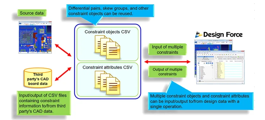
It is important that constraints can be attached to full so-called electrical nets (including series passive components like capacitors and resistors), and as well for groups of nets (e.g., buses or net classes) rather than just on a single particular net. Inheritance in constraining speeds up the process too. All this is a key advantage in the constraining process, as defining constraints for larger systems can then be carried out much faster. Constraints can be reused by importing/exporting as constraint templates (net topologies) or in standard formats such as .XML or .CSV.
Learn more about PCB constraint management in our on-demand webinars


- Blog
Modern electronic products are no longer built around a single PCB. As systems become faster, denser, and more interconnected, engineering teams are being forced to rethink how they design, verify, and manage complex multi-board products.

- Blog
Explore how CR-8000 enhances PCB design with integrated control of impedance and resistance—enabling precise analysis for both high-speed and high-power applications, from signal integrity to power distribution optimization.

- Blog

- Blog
AI in PCB design is increasingly seen as a game-changer, with some predicting it could soon replace entire layout teams—but this view risks overlooking both the current limits of AI and the critical expertise engineering demands. At DesignCon 2025, experts from emphasized that AI's real value lies in complementing human judgment, not replacing it. Read more on our blog.
- Webinar
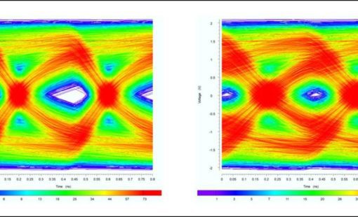
Using the example of the analysis of SerDes transmission paths such as PCI Express, SATA or USB3, we explain the methodology of an analysis- and constraint-driven assembly development with CR-8000 Design Force.

- Webinar
In this webinar the use of the Rule Stack Editor and Clearance Class in conjunction with the Constraint Browser will be explained step by step.