
Growing Pains in the Wearables Market
By 2020, the wearable tech market is expected to grow to around $34 billion with sales of roughly 411 million devices, according to industry analyst firm CCS Insight. Capturing your share of these revenues will require delivering ever-increasing functionality in smaller and lighter devices which will often require contoured form factors to accommodate style considerations and match the shape and movement of the human body.
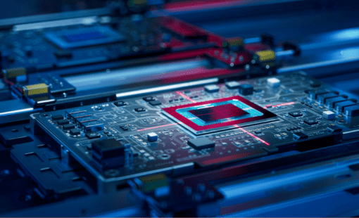
Most wearable manufacturers have determined that the only current way to meet these often-conflicting goals is to ramp up their use of advanced packaging technologies such as Multichip Module (MCM), System in Package (SiP) and 3D-IC in order to pack integrated circuits more closely together. Flex PCBs are increasingly being used to reduce enable the use of more stylish aerodynamic shapes.
With key functionality in many cases commoditized, the success or failure of wearables is increasingly determined in the early stages of the PCB and mechanical integration process where requirements are translated into practical design decisions such as how functions are mapped to PCBs and PCBs are integrated into the enclosure. These decisions determine cost, size, weight and external appearance and other outcomes. The problem faced by designers is that today’s leading design tools largely fail to address this critical early stage of the design process and instead focus on later stages where the detailed design is defined. The failure to choose the right options in the early phases can result in expensive late-stage changes or even a product that fails in the market.
Zuken is helping engineers overcome these challenges by providing a virtual prototyping environment where the product can be configured and decisions made such as how many boards will be used and what functions will be assigned to each board. For each design alternative, the new tool helps evaluate the cost, number of PCBs, weight, size, enclosure fit and more with the ability to make tradeoffs before committing to a detailed design. There’s far too much to explain in this short blog post so we wrote this article that provides full details on the new generation of design exploration tools.

-
Chief Strategy Officer


- Blog
Executives’ Perspectives on Digital Transformation #6

- Blog
Modern electronic products are no longer built around a single PCB. As systems become faster, denser, and more interconnected, engineering teams are being forced to rethink how they design, verify, and manage complex multi-board products.

- Blog
Executives’ Perspectives on Digital Transformation #5
- Blog
Explore how CR-8000 enhances PCB design with integrated control of impedance and resistance—enabling precise analysis for both high-speed and high-power applications, from signal integrity to power distribution optimization.
Related Content

- Products
CR-8000 is a System-Level PCB & IC Package Design software including 3D Multi-board, Analysis and MCAD Integration

- Blog
Since it contributed to making the iPhone 7 even thinner than its predecessors, fan-out wafer-level packaging (FO-WLP) technology has risen in the collective consciousness. By adopting FO-WLP on this scale, Apple sent out a signal that though highly novel, the technology had matured.