Support for multi-board design and extraction of multiple PCB netlists from one schematic
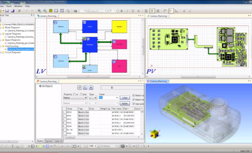
PCB Design Creation - Design Gateway is a platform for logical circuit design and verification of single and multi-board system-level electronic designs. It supports a true system-level circuit design in which individual circuits can be represented and connected as blocks. The platform enables engineers to manage signal continuity (interconnects) at the system level rather than just at the design level, allowing for an evaluation of board-to-board signal continuity.
Support for multi-board design and extraction of multiple PCB netlists from one schematic

Interface with best-in-class simulation tools for analogue/mixed signal, RF, and system level analysis

"What-if” studies to determine best termination and topology of critical signals

Parallel use of black box symbols and parts to enable initial layout early in the design process
PCB Design Creation – Design Gateway brings extensive design, simulation and analysis capabilities to your desktop. It allows companies to manage and make optimal use of engineering design data across all company and team sites. Intelligent multi-board design is inherently supported in Design Gateway.
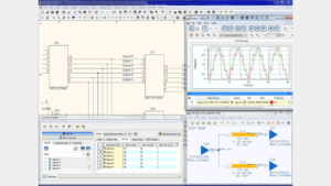
The platform provides complete system circuit engineering. Native and interactive integration with a wide range of signal integrity (SI), analogue, digital, and multi-technology verification tools is provided. Through this it also supports the co-simulation of analogue and digital functional blocks and programmable devices. Design Gateway enables design re-use, allowing engineers to use proven and tested logical circuits from previous projects
How to manage signal continuity (interconnects) at the system level in a compact 1:20 min overview
A complete solution for the design and verification of single and multiboard systems
PCB Design Creation – Design Gateway allows you to design a true system-level circuit design by creating a board-level block or connector symbol for each individual circuit, and connecting them together to define a complete system. Engineers can avoid maintaining spreadsheets of system interconnects, and manage them with intelligent graphical design. With the power of the multi-board design technology in Design Gateway, you have the option of selecting each board symbol and generating a netlist for each PCB, or create a full system-level netlist to support the complete analysis of a product.
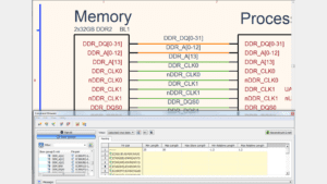
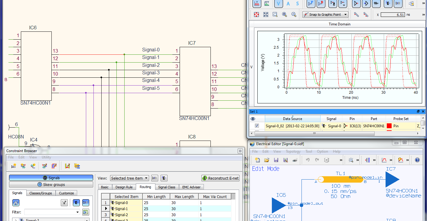
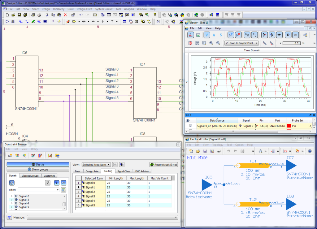
Whether you are challenged with the complex requirements of DDR2/3/4 or faced with incorporating the latest high-speed interfaces, the Constraint Browser within Design Gateway enables you to define constraints for any combination of nets, extended nets, differential pairs, and busses using a spreadsheet approach. In the same instance, a user can continue adding layout rules for nets and manage complex spacing rules within net groups and between net groups.
With embedded simulation and verification, and flexibility to interface with best-in-class tools, Design Gateway reduces errors and improves your design cycle time by utilizing the same schematic for both PCB layout and simulation. Whether you require analog or digital simulation, verifying polarized capacitors are connected correctly, or insuring that the simulated signal voltage doesn’t exceed power ratings of a component, you can accomplish all this in a co-design flow using Design Gateway.
The benefits of design reuse are well-known, but implementing a methodology that is flexible, easy to use, and can take advantage of data management was not fully realized until Design Gateway. Design Gateway introduces a flexible approach that allow you to design with certified circuits, use a circuit from an existing design as a template for a new design, or creating a multi-PCB design – using either a top-down or bottom-up approach. Block circuits can be saved in a library for you to catalog and search and add to a design. Revision control can be used to govern any changes to a circuit – all part of Design Gateway’s robust approach to block circuit management.
The following can be added to extend the functionality of CR-8000 Design Gateway
A simulation cockpit for Spice simulation tools (PSpice, LTSpice, HSPICE)
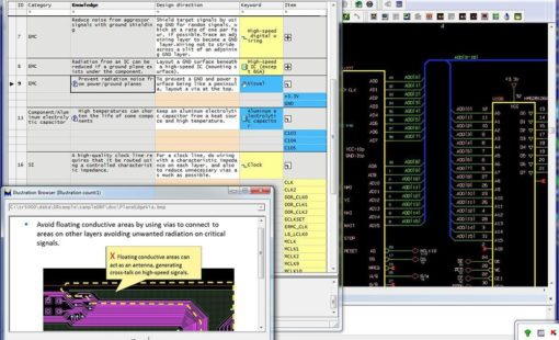
Circuit DR-Navi helps design teams consolidate engineering expertise and best practices into a central knowledge base integrated with the design process. During logical circuit design, engineers can access a standard set of requirements or create project-specific instructions to drive design guidelines across the PCB design flow.
Graphical Pin Manager (GPM), offers an effective FPGA/PCB co-design environment providing support for the latest devices offered by FPGA vendors, such as Xilinx, Altera, Lattice, and Microsemi.
Design Gateway’s Circuit Adviser enables engineers to conduct concurrent, advanced electrical rule checks during logical circuit creation. Users can specify rules and conditions, create check results, cross-probe results with the design and generate summary reports.
Design Gateway Viewer is a native schematic data viewer with comprehensive analysis capabilities, such as cross-probing, constraint viewing, signal classes and many more.
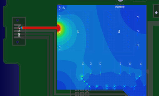
Scenario EX enables to check the electrical characteristics and the connection topology of signal tracks. It allows “What-If Scenarios” of both schematic and layout data to optimize the behaviour of a circuit. It can be used both for interactive design and design verification.
System Planner provides a system-level design environment for the architectural planning and optimization of electronic systems and products. It enables engineers to optimize partitioning and performance of multi-board systems and maximize design reuse, while eliminating the need to re-enter up-front planning data into the design tools during detailed design.
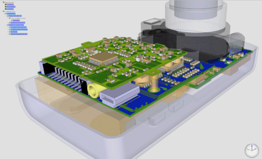
Design Force combines traditional 2D design with native 3D design and the latest human interface techniques, accelerated graphics and almost instantaneous rendering and refreshing. It is the fastest, most effective PCB design solution available today. Design Force enables design teams to layout their designs in the context of a complete system or product.
Find out more via our webinars, blogs, press releases and more...
See how CR-8000 Design Gateway addresses the most challenging design tasks
Design Gateway provides complete system circuit engineering. Native and interactive integration with a wide range of signal integrity (SI), analog, digital, and multi-technology verification tools is provided. Through this it also supports the co-simulation of analog and digital functional blocks and programmable devices.