Tech-Tip: Compare the shape of each layer in two design data items
The Designer can compare two designs to see the differences between the two. This can be useful if minor changes or major changes have been made to an existing design or one received from another facility.
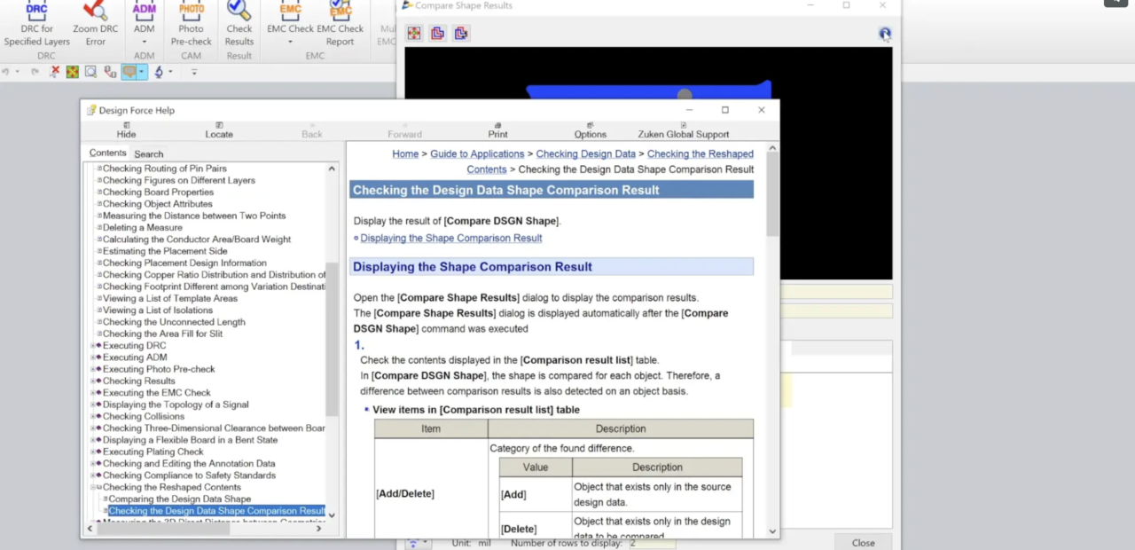
Two compared design data items are overlapped on the canvas.
The currently opened design data on the canvas of the main window is handled as the comparison source, and the design data specified in [Target file] with the [Compare DSGN Shape] command is done as the comparison destination.
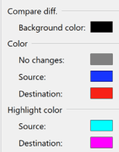
The design data side of the comparison source is displayed in the color specified in [Application Settings] – [Compare diff.] – [Color] – [Source].
When a difference found in the design data side of the comparison source is selected from [Comparison result list], it is displayed in the color specified in [Highlight color] – [Source].

-
Applications Engineer


- Blog
Explore how CR-8000 enhances PCB design with integrated control of impedance and resistance—enabling precise analysis for both high-speed and high-power applications, from signal integrity to power distribution optimization.

- Blog

- Blog
AI in PCB design is increasingly seen as a game-changer, with some predicting it could soon replace entire layout teams—but this view risks overlooking both the current limits of AI and the critical expertise engineering demands. At DesignCon 2025, experts from emphasized that AI's real value lies in complementing human judgment, not replacing it. Read more on our blog.

- Blog
Our new post explores the potential of augmented reality (AR) to transform everyday experiences in shopping, education, and navigation. It highlights how enhanced AR devices will offer immersive, interactive environments that blend the virtual and physical worlds.
