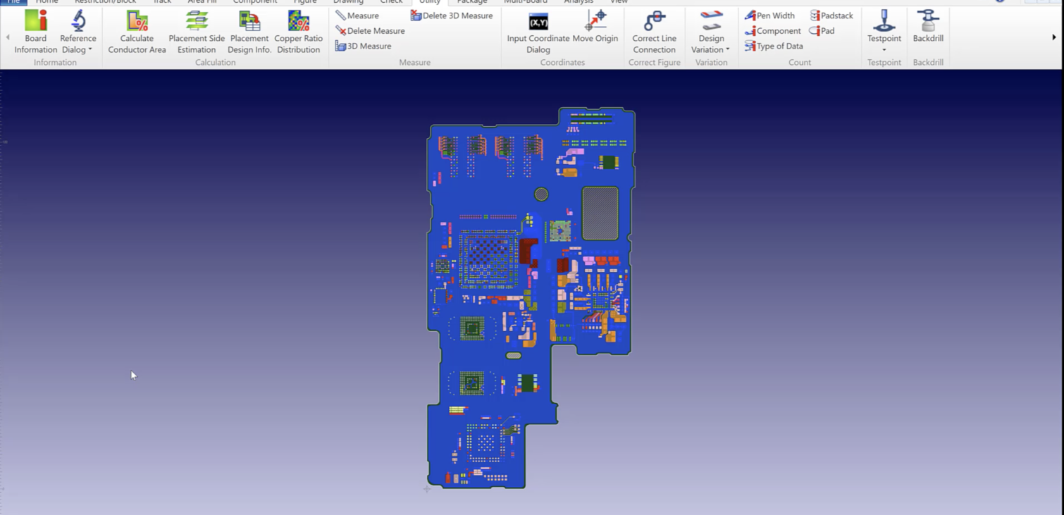
Tech Tip: Reporting All Wire Widths by Layer using CR-8000 Design Force
Menu
Engineers have been asking is it possible to get a report of the wire width for each routed trace by layer the answer is yes. Using CR-8000 Design force an Object Filter can be created to select only traces on each layer and then a report can be shown reflecting the information using the utility “Pen Width”. This gives the Engineer a quick way of reporting the number of traces and their width for each conductive layer. Below is a video demonstration.

-
Applications Engineer

Jeff Perry is a Customer Support Applications Engineer. He focuses on customer support for CR-5000/CR-8000 Tool Suites. Jeff provides instruction on Zuken tools at customer sites or via the web. He also puts together Application Notes, Tool Tips and Tech Tips which help improve customer productivity. He enjoys golf and spending time with his grandson.
- Blog
September 10, 2026
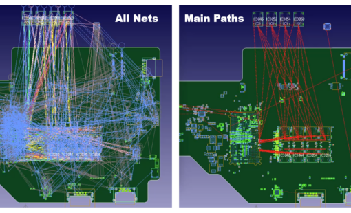
Tech Tip: PCB Net Visualization with CR-8000’s Main Path View
cr-8000, Tech-Tips, CR-8000, CR-8000 Tech Tip, Net Visualization, Path View, Tech Tip, Blog

- Blog
August 20, 2026
Phased Array PCB Design: Beamforming and Engineering Considerations
cr-8000, Electronic, PCB Design, Antenna Design, Beamforming, Controlled Impedance, CR-8000, Design Reuse, PCB design, Phased Array, Power Integrity, RF Design, Signal Integrity, Thermal Management, Blog
- Blog
July 16, 2026
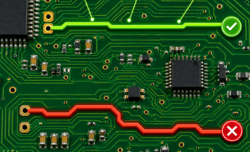
Tech Tip: Check PCB Trace Resistance with Ohmic Distance in CR-8000
cr-8000, Electronic, PCB Design, Tech-Tips, Constraint Management, CR-8000, CR-8000 Design Force, CR-8000 Tech Tips, Design Verification, High-Current PCB Design, Ohmic Distance, PCB design, PCB Engineering, pcb layout, PCB Trace Resistance, Power Integrity, Signal Integrity, Tech Tips, Blog
- Blog
May 14, 2026
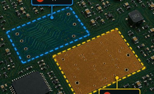
Tech Tip: Precise PCB Keepout Area Control with CR-8000
cr-8000, PCB Design, Uncategorised, CR-8000, CR-8000 Design Force, PCB, pcb layout, Blog
Related Products & Resources
- Blog
September 10, 2026
Tech Tip: PCB Net Visualization with CR-8000’s Main Path View
cr-8000, Tech-Tips, CR-8000, CR-8000 Tech Tip, Net Visualization, Path View, Tech Tip, Blog
- Blog
August 20, 2026
Phased Array PCB Design: Beamforming and Engineering Considerations
cr-8000, Electronic, PCB Design, Antenna Design, Beamforming, Controlled Impedance, CR-8000, Design Reuse, PCB design, Phased Array, Power Integrity, RF Design, Signal Integrity, Thermal Management, Blog
- Blog
July 16, 2026
Tech Tip: Check PCB Trace Resistance with Ohmic Distance in CR-8000
cr-8000, Electronic, PCB Design, Tech-Tips, Constraint Management, CR-8000, CR-8000 Design Force, CR-8000 Tech Tips, Design Verification, High-Current PCB Design, Ohmic Distance, PCB design, PCB Engineering, pcb layout, PCB Trace Resistance, Power Integrity, Signal Integrity, Tech Tips, Blog
- Blog
May 14, 2026
Tech Tip: Precise PCB Keepout Area Control with CR-8000
cr-8000, PCB Design, Uncategorised, CR-8000, CR-8000 Design Force, PCB, pcb layout, Blog