
Pre-Layout Analysis for High-Speed Design, Part 1
In my last post, we discussed the big picture of high-speed design analysis phases. In this post, we will discuss the first phase, pre-layout analysis for high-speed design.
Pre-Layout Analysis
During system planning and circuit design, it is important to evaluate whether our designs are producible, stable, and cost-effective, especially when working with high-speed PCB designs.
With high-speed PCB designs, we know that the connected wires become the transmission-lines. In other words, the electrical functions might not be established even if we connected the traces from one end to another.
In the pre-layout analysis phase, we will focus on solving the following issues:
- Could we implement the concept from the system and circuit designs into a real product?
- How stable will the product be?
- How cost-effective is the product versus its performance and functionality?
Design Producibility
High-speed PCB designs may face new challenges due to transmission lines, fast signal switching rates, and small product size (portable and miniature). From a signal integrity point of view, an engineer needs to make sure the product can be producible while retaining its required functionality. To achieve this, EDA tools must provide a topology builder, along with simulation capabilities.
Product Stability
Stability verification is an essential task in the post-layout phase that we will discuss later. But to start, stability simulation is critical in the pre-layout analysis phase. For example, we might find a different set of chips that works more stable than our original selection. Or we might identify a particular via structure to help improve the signal qualities. Pre-layout signal integrity simulation and error bit analysis help mitigate the stability issues found after PCB layout.
Cost-effectiveness
The overall cost of a product includes design cost, material cost, process cost, and manufacturing cost. High-speed design analysis can help the designer select more functional parts, cheaper components, easier production processes, and more reusable product blocks. Similarly, what-if simulation plays a vital role in analyzing a product’s cost-effectiveness by making sure it can maintain a good ratio of cost, stability, and functionality.
CR-8000 Pre-Layout Analysis Capabilities
Zuken’s CR-8000 tool suite covers all the necessary functionalities for the pre-layout analysis phase. Both CR-8000 Design Gateway (schematic design) and CR-8000 Design Force (PCB and package layout) link to the CR-8000 Electrical Editor for concurrent analysis. CR-8000 can verify a design’s producibility while enabling what-if analysis to improve cost-effectiveness and stability.
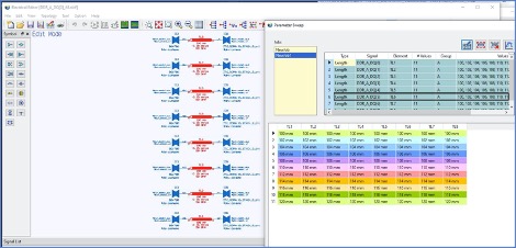
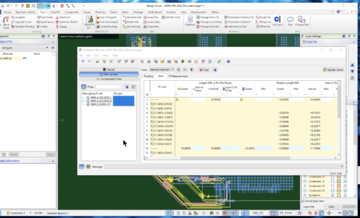
This video shows how Electrical Editor seamlessly extracts a schematic net from Design Gateway; how to change the topology structure for the DRR4 clock nets; and how to use the Conductor Configuration Manager parameter sweep feature for trace layout planning.
CR-8000 Electrical Editor can sweep the parameters for trace width, distance, thickness, etc. It can also sweep the trace length for part spacing and route length planning.
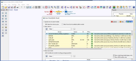
Electrical Editor can also perform component what-ifs by swapping the component models to identify the most reliable and cost-effective part solutions for product manufacturing.
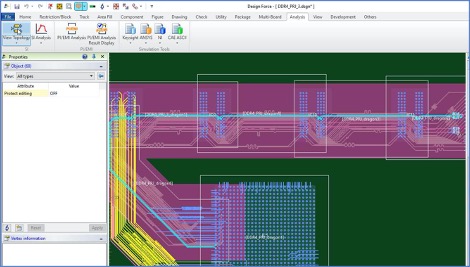
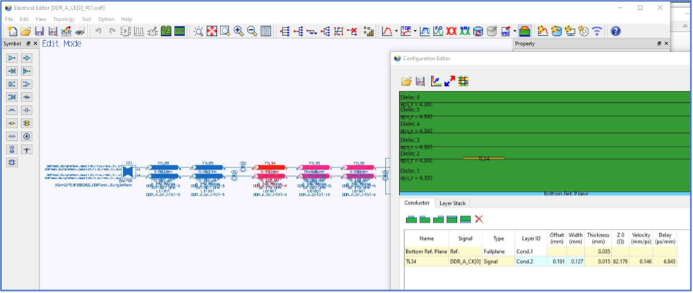
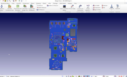
CR-8000 Design Force also contains embedded pre-layout analysis features. The most significant advantage of performing pre-layout analysis in Design Force is the ability to extract nets that contain the layer stack information. As a result, the engineer can use the layer stack information as a reference for more accurate PCB layout planning.
Conclusion
To sum up, the pre-layout analysis phase is valuable for early-stage product design verification and for improving product functionality and stability. Most importantly, this phase can increase a product’s profitability by improving its cost-effectiveness.
Zuken’s CR-8000 tool suite provides many pre-layout analysis functionalities from schematic to PCB layout. So, understanding the pre-layout phase with CR-8000 capabilities can help you speed up the design process, improve product quality, and reduce process and manufacturing costs.
In part 2 of this series, we will discuss the constraint-driven methodology and applications in the pre-layout analysis phase. Stay tuned!
References:
-
High-Speed PCB Design Analysis Phases and Constraint-Driven Methodology, Lance Wang
https://www.zuken.com/us/blog/high-speed-pcb-design-analysis-phases-and-constraint-driven-methodology/ - High-Speed Digital Design Flow, Keysight
https://www.keysight.com/main/editorial.jspx?cc=US&lc=eng&ckey=1963655&id=1963655 -
The Basic Signal Integrity Simulation Tasks You Should Perform, ZM PETERSON
https://www.nwengineeringllc.com/article/the-basic-signal-integrity-simulation-tasks-you-should-perform.php -
What’s The Difference Between Pre-Layout And Post-Layout PCB Simulation? Patrick Carrier
https://www.electronicdesign.com/technologies/boards/article/21795766/whats-the-difference-between-prelayout-and-postlayout-pcb-simulation

- Blog

- Blog
- Blog
- Blog
Related Products and Resources

- 2020 Technical Webinars
This webinar will explore a high-speed design process in CR-8000 that utilizes a constraint browser, topology template, crosstalk estimation, signal and power integrity simulations.

- 2020 Technical Webinars
In this session, we will review some of the new features that have been added in the CR-8000 Design Force and offer some explanation of how these additions will benefit our customers within their design flows.