Flex PCB Design for Cost-effective Panelization
The Printed Circuit Board (PCB) market continues its steady growth. Spearheading that growth is the Flex PCB (FPC) sector. Many researchers predict the FPC market will grow more than 10% year-over-year in the coming decade.
Flex PCB design is clearly not a new technology; it has been around for decades. Thanks to the relentless efforts and innovations of material and board suppliers, the FPC technologies are evolving rapidly and replacing cables and rigid PCBs in many design applications. Consequently, the more FPCs included in a product design, the more critical their cost becomes, no matter the industry. This is especially true for high volume, mass production situations such as consumer products.
Flex PCB Design and Design for Manufacturing
Taking design for manufacturing (DFM) requirements into consideration during the design process offers an opportunity to improve the flex PCB design quality and overall efficiency for hardware engineering. At the same time, it helps reduce iterations in the manufacturing change request process. CAD and DFM check systems continue to evolve to keep up with emerging technologies. But is it early enough to account for the FPC manufacturing costs?
This question was the primary motivation for exploring the various measures to reduce FPC manufacturing costs. The question also gave rise to interest in exploring design for panelization (DFP).
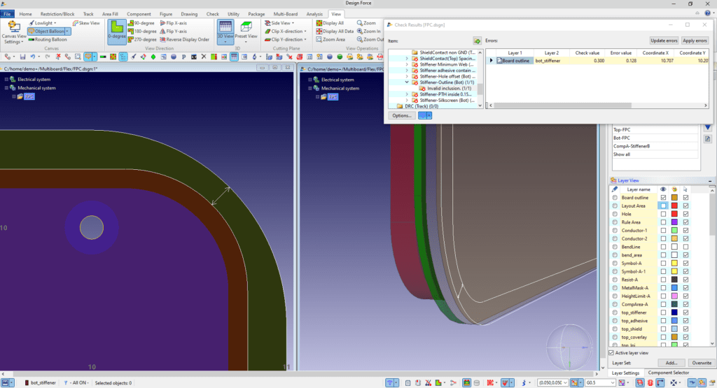
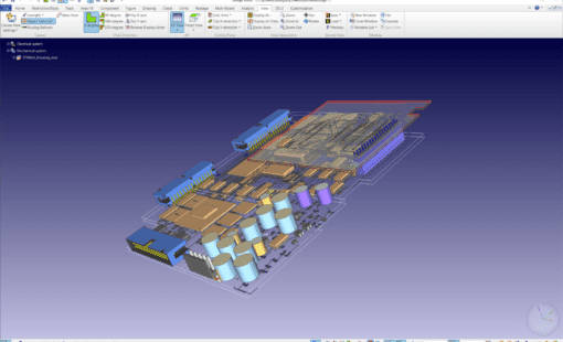
As a side note, Zuken’s Advanced Design for Manufacture (ADM) tool also offers benefits in the FPC arena. It is a GUI-based engine for creating complex DFM checks. The tool allows for precise DFM rule creation that addresses areas of concern unique to the FPC realm. But that’s a topic for a later post.
Optimizing PCB Panelization
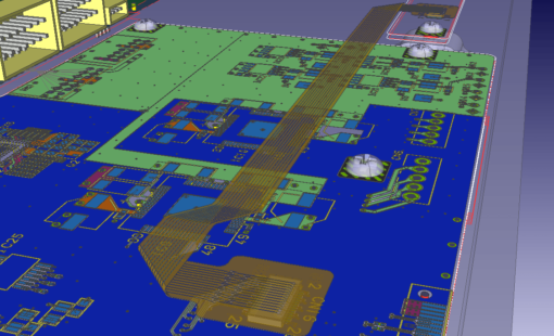
The proven and cost-effective single-sided flex PCB is in wide use today. Yet the demand for the complex FPC–double-sided, multi-layer, and with new materials such as LCP (liquid-crystalline polymers)–is steadily increasing. As you can easily imagine, both the manufacturing costs and material costs for complex Flex PCB design are relatively high. As a result, managing the various cost factors is vital for competitive product design and manufacturing. Applying DFM checks early during the PCB design process can improve efficiency by reducing the iterations (time and labor) between design and manufacturing. But note that it is also essential to reduce the direct material cost of the FPC by improving the material utilization to maximize the cost-efficiency.
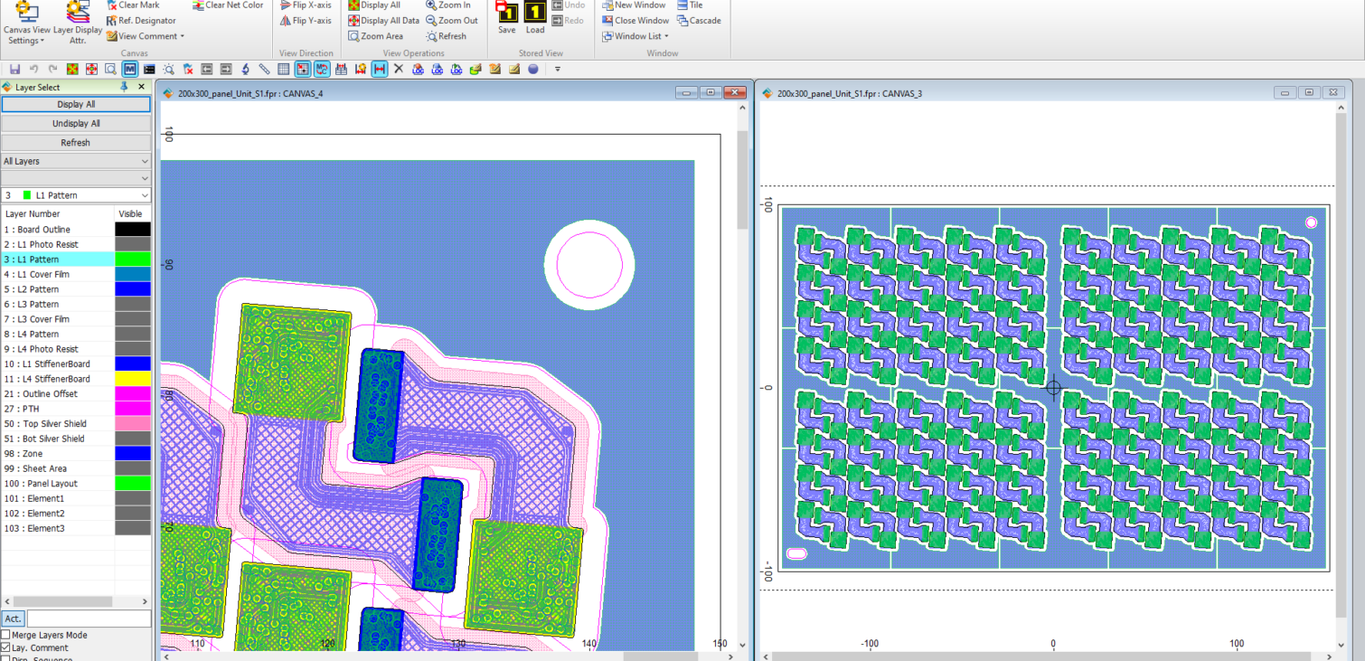
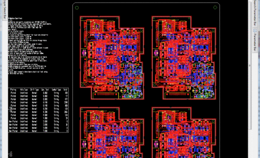
Reducing material costs is more critical for complex FPCs and high-volume mass production. One of the most impactful methods to achieve cost reduction is to improve the utilization of materials on production panels. In other words, the more boards you can squeeze into a given space, the cheaper the board will be. As this is so critical and a direct cost-saving factor, suppliers often rely on specialists to design the FPC panel. Those specialists carefully design the panel layout to optimize space and materials utilization. They consider several factors such as manufacturing tool/jig units, molds, cutting dies, film sealing, and of course, the manufacturing capabilities of the production lines. But the element with the most significant impact on panel utilization is the board shape, which is determined in the very early phases of the product design.
Design for Panelization
Simply speaking, the effect of an optimized board shape trickles down and ultimately affects material costs. It is critical to design the board shape with consideration for the panel layout utilization. But how do you make this happen? Before going further, let’s reconfirm the general assumptions for the flex PCB design and manufacturing process, focusing on design for panelization (DFP) and the cost savings it can create.
General assumptions:
- Flex PCB designs are produced as panels, and each FPC board is laid out in a specific pattern with a specific pitch in the panel, known as “Step and Repeat.”
- Unlike a rigid PCB assembly panel, FPC boards can be laid out at any angle if they are in a regular pattern to enable efficient repeating of the manufacturing process unit (e.g., mold cut and film lamination). So, completely irregular layout patterns are prohibited for efficient processing.
- Meanwhile, you must maintain a certain spacing for manufacturability (e.g., board to board = 1.5mm, X panel edge margin = 2mm, Y panel edge margin = 3mm).
- A given panel size with a given FPC configuration (i.e., stackup) has a fixed unit cost.
- For example, 1 square meter of a double-sided FPC panel with silver shield and coverlay films on both sides, with component placements in one region on the top side (i.e., FR4 stiffener on the other side and LPI mask on the top side) may be $200. This unit cost won’t change regardless of the number of boards per square meter.
- In other words, the more boards per square meter, the cheaper each flex board will be.
- Changes to the board outline are possible in the early design phases, but not later.
- Product engineers (system architects or mechanical engineers) likely own this phase. This phase would be very early, or even before the PCB design phase.
Conclusions:
- Optimizing the board shape will improve the panel efficiency.
- The board shape cannot change once the design is fixed. So, optimization needs to happen in the early phase.
- Adding a new step in the early phase must be quick and straightforward for system architects, product engineers, or even mechanical engineers to optimize the design and conduct what-if analysis.
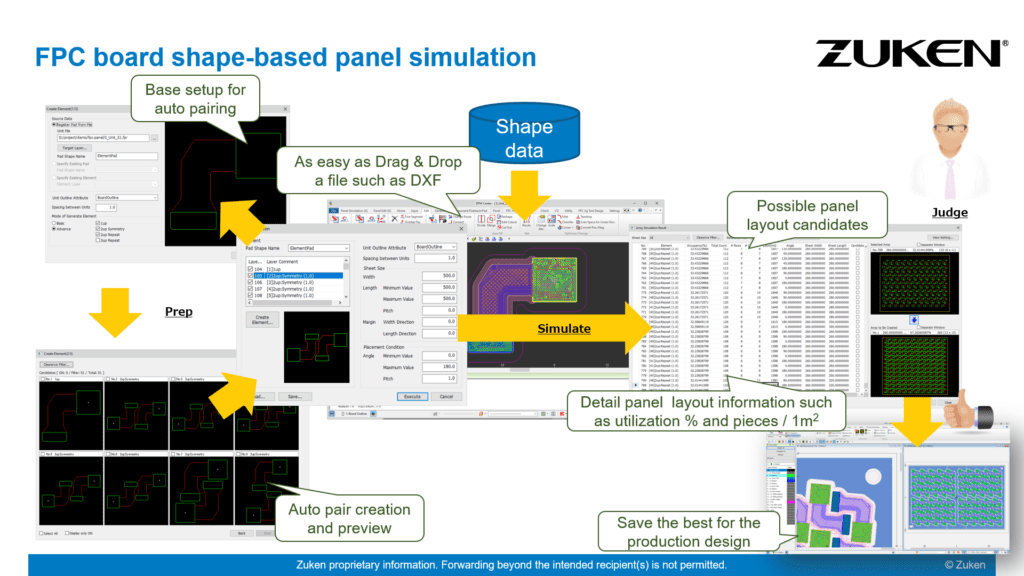
Getting back to the question at hand, how do you design the board shape while considering panel layout utilization? Using an advanced, automated design solution is the answer. Zuken’s CR-8000 DFM Center is a tool typically used among board suppliers for CAM design. But it also has a utility called FPC Panel Simulation Module. Initially developed for the panel design specialists at the flex PCB suppliers, this utility makes quick work of what-if panel configuration simulations. System engineers can also use it for design for panelization optimizations to the board profile. CR-8000 makes it easy to drag and drop, then simply push a few buttons to run through the thousands of panel layout patterns to validate the utilization data points and actual panel layout–all in a matter of seconds or minutes (*1). Accurate reports can be reviewed to quickly determine the density and PCB count to weigh in the decision-making process.
In reality, it is also essential to consider other cost factors. These can include differences in labor cost depending on where the boards will be built and the running and maintenance cost of the flex PCB production equipment. However, it is also fair to assume that optimized panel utilization will improve cost efficiency in these areas.
Reducing Costs for Customers
Zuken created this tool based on an expressed need from our customer base. Reducing the costs of our customers’ products is an area of great importance and drives much of our development effort. Customers realize significant benefits in running through multiple panel configurations to ensure an ideal panelization arrangement early in the design process. In addition, designers can use the tool to weigh different FPC shape options against each other to confirm the perfect final form. By optimizing the flex PCB shape and panelization configuration, we can ensure that every possible cent is saved in the customers’ final products. We are happy to share this new flex PCB design for panelization approach and explore your potential cost savings. Please contact us for more details.
*Depending on the board shape and simulation parameters.
Learn more about how to improve Flex PCB design manufacturing productivity with better DFM checks in our on-demand webinar

-
Engineering Team Manager, SOZO Center

- Blog

- Blog
Related Products and Resources
- Products
- Products
PCB Design for Manufacturing (DFM) enables designers to handle the increasing complexity and diversity of today’s PCBs, while ensuring high final product quality, and accurate outputs for the manufacturing processes. With a robust set of features for data preparation and embedded verification to ensure manufacturing specifications are met...