A Primer on Wide Bandgap Semiconductors and Power Supply Decoupling
Wide Bandgap Semiconductors: The Future of Power Electronics
In the world of power electronics, there are few buzzwords thrown around more than wide bandgap semiconductors. These new devices promise smaller, more powerful, more efficient power electronics devices than we’ve ever seen before. Many industrial power supplies already incorporate wide bandgap (WBG) semiconductors. Projections show that in time, that trend will expand into the consumer electronics market. Mobile device chargers already use wide bandgap semiconductors. The wide bandgap variant of these chargers permits fast, high-current charging without the need for large wall warts. Designing devices with wide bandgap semiconductors may appear trivial, but it can often be difficult to leverage the full benefits of this new technology. Thankfully, the industry offers reference designs to help get designers off to a strong start. And ECAD tools like eCADSTAR provide the necessary features to implement one of these designs successfully.
Valence and Conduction Bands
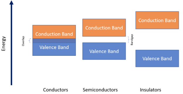
We’re not going to get into quantum field theory and all that mind-bending stuff around whether electrons are particles or waves, then get lost in a Heisenberg/Schroedinger soup. Not today. For the sake of argument, let’s use the simple planetary model of an atom. In simple terms, the valence band is the highest energy level at which unexcited electrons lie. The bandgap is the amount of energy required to make electrons jump to the so-called conduction band, where the material becomes electrically conductive. Using this model, we can organize materials into three categories:
- Conductors – Materials with a tiny, easy-to-cross bandgap, like metals, which are highly electrically conductive.
- Semiconductors – Materials with a narrower bandgap but with sufficient additional energy; the electrons can cross the bandgap and become electrically conductive.
- Insulators – Materials with much wider bandgaps that will not conduct electricity without breaking down completely.
Wide Bandgap vs. Conventional Silicon
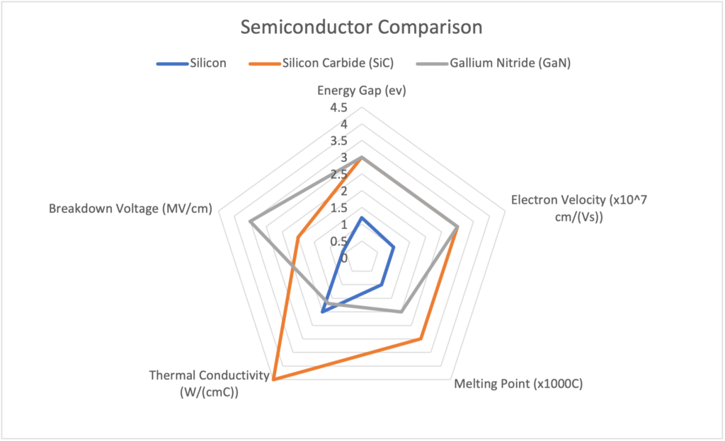
Traditional silicon used in most modern electronics has a bandgap of around 1eV. This makes the silicon usable for about 600V with higher voltages possible if the size of the PN junction is also increased. . Wide bandgap materials such as gallium nitride (GaN) and silicon carbide (SiC) have nearly three times as much bandgap energy but can still be conductive. Using WBG materials results in devices that can easily operate around 1700V.
These materials are also known as high electron mobility transistors (HEMTs). All that means is that the speed at which charge carriers move through the lattice is relatively high. Therefore, the devices can switch at relatively high frequencies and have low conduction losses. Both properties are desirable because they enable smaller, more efficient devices.
Switchers and Wide Bandgap
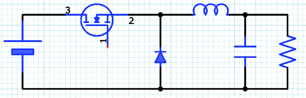
When it comes to power electronics, we primarily find WBG devices in use in switched-mode power supplies (SMPS). Semiconductors in power electronics can be used to create voltage regulators that attempt to keep the voltage constant despite changing load conditions. Using WBG semiconductors in the power stage of these devices generates the final output voltage that drives downstream electronics. Other controls circuitry such as gate drivers and logic still use conventional silicon. The WBG transistors control the flow of current between the passive elements of the regulator.
The nature of an inductor is to resist changes in current. Capacitors, on the other hand, resist changes to voltage. When the transistor turns on, current flows into the inductor, creating a voltage that counteracts the source voltage. The resulting voltage is lower than the source. When the transistor turns off, the inductor becomes the current source and the output capacitor stores and smooths that energy so that the load can use it. The topology, device selection, and switching scheme are all determining factors in the operation of the regulator.
Decoupling Networks
Decoupling networks consist of capacitors used in a bypass configuration between a supply and ground. Although these capacitors play a dual function–it really is the same–they supply energy when needed in cases of elevated demand, and they filter noise. The impedance profile of a decoupling network is critically important to how it operates. Usually, a low impedance is most desirable across the band of frequencies that need to be filtered out and shunted to ground. How low the impedance needs to be depends on the amplitude of the noise in question. Usually, under 100mΩ is a good guideline. The size, values, and quantity of capacitors in a decoupling network all impact the impedance profile.
Keeping Inductive Loops Short
Designing an effective SMPS is not just about component selection and parametrics. The design of the layout itself is also has a significant impact on performance. It is necessary to maintain short return current loops to prevent additional ringing during switching events and transients. The mutual inductance of copper traces can add an undue amount of total inductance to the circuit. With this in mind, it’s essential to have sufficient ground via stitching and close proximity of placement devices.
ECAD Tools to Facilitate the Process
The more complex our devices get, the harder it becomes to implement these new technologies successfully. Many device manufacturers try their best to provide support and guidance to engineers to help them succeed with their designs. The reference designs offered by manufacturers offer guidelines to achieve many successful implementations. It is up to engineers to balance design constraints and desired performance to hit their targets. ECAD tools such as eCADSTAR help engineers evaluate these tradeoffs and arrive at the most effective design for their needs. eCADSTAR enables quick adoption and integration of new componentry, provides simulation and validation tools, and facilitates sending a design to manufacturing so that designers can succeed. The see this in action, check out the webinar on Optimizing the Decoupling Network for a GaN-based Switcher.

- Blog

- Blog

- Blog

- Blog