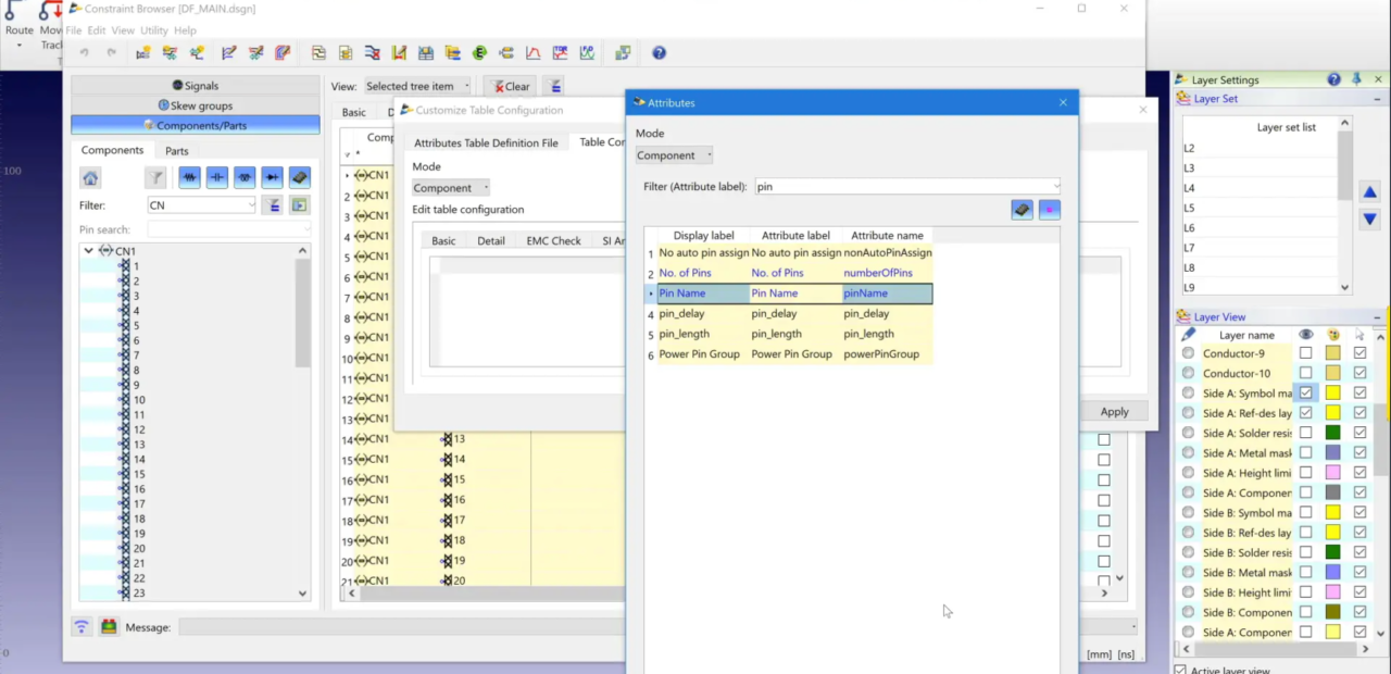
Tech-Tip: Creating a Connector Pin Netlist
Checking the pinout of your connectors is an important part of creating your printed circuit board. Checking your pin connections can save you from a costly re-spin of your circuit board. This can be done using the Constraint Browser in Design Force. By default, the Constraint Browser does not show this information.
To create the view needed you must use the Customize Table Configuration. Add a new tab to the spreadsheet view of the Constraint Browser. Once you have added the new tab you can set the filter to only show connectors in the tree view. Afterward, expand all of the Child items, and select all of the pins to be visible in the spreadsheet view. This can be selected, copied, and pasted into an excel spreadsheet.
Check out all of our Tech Tips here!

-
Applications Engineer


- Blog
Modern electronic products are no longer built around a single PCB. As systems become faster, denser, and more interconnected, engineering teams are being forced to rethink how they design, verify, and manage complex multi-board products.
- Blog
Explore how CR-8000 enhances PCB design with integrated control of impedance and resistance—enabling precise analysis for both high-speed and high-power applications, from signal integrity to power distribution optimization.

- Blog

- Blog
AI in PCB design is increasingly seen as a game-changer, with some predicting it could soon replace entire layout teams—but this view risks overlooking both the current limits of AI and the critical expertise engineering demands. At DesignCon 2025, experts from emphasized that AI's real value lies in complementing human judgment, not replacing it. Read more on our blog.
Related Content
- Products
CR-8000 Design Force is the fastest, most effective PCB design solution available today. Design Force enables design teams to layout and verify their designs in the context of a complete system or product.

- Products
CR-8000 is a System-Level PCB & IC Package Design software including 3D Multi-board, Analysis and MCAD Integration