
Determining Conductor DC-Resistance in CR-8000 Design Force
Electrical Parameters at your Fingertips
Menu
 In a simplified view, engineers often tend to assume that PCB conductors behave perfect with zero resistance and no energy loss or dispersion, but in reality this is not the case.
Instead, PCB designers working on high-speed or RF designs have to deal with impedance from an early stage — trace impedance in particular — and more recently also power-plane impedance, but seldom thought on resistance quantities in particular This particular emphasis on impedance has created the situation that the layout engineers as a consequence often struggle with the relation between trace copper resistance, impedance, and reactance.
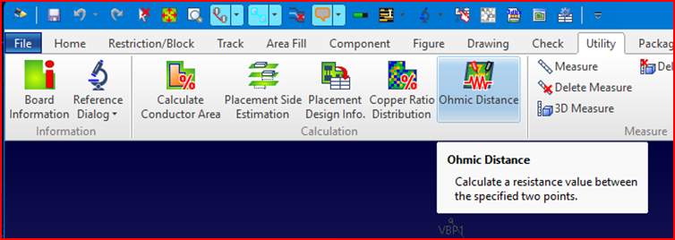
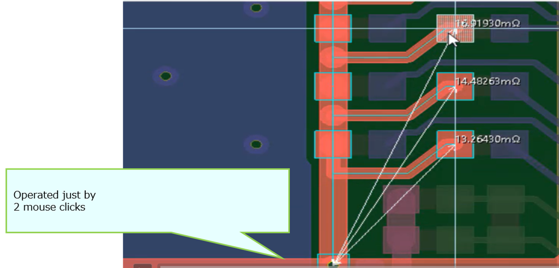
To address this and to provide engineers with an as easy as possible solution in their design flow, Zuken has recently added a new capability to CR-8000 Design Force—utilizing a new EM solver—for the fast but highly accurate computation of the point-to-point DC resistance within a selected copper structure (signal nets or power nets including copper poured structures).
The result is displayed immediately in the Design Force canvas but also listed in the Constraint Browser for the net-entities. The key aspect in implementing this feature was to give layout engineers access to relevant electrical parasitic figures of their PCB structures in an easy yet highly accurate manner.
Background: Resistance vs. Impedance
Both, trace impedance and trace resistance are closely related to each other and both relevant for PCB designers. Impedance is a complex-valued quantity consisting of resistance (real part) and reactance (imaginary part) of a PCB trace.
At DC, a PCB trace behaves as a resistive element with its well defined DC resistance. Reactive effects arise only at higher frequencies due to parasitic inductance and capacitance.
Sometimes, especially for engineers entering the world of impedance-controlled signals, there can be confusion when interpreting the requirement documents—assuming a resistance target where in reality an impedance target must be met. CR-8000 supports this through its integrated field solver and impedance-controlled routing and constraining capabilities, particularly for high-speed signals.
However, there are cases where knowing the DC resistance of a trace or conducting area is essential—for example in power delivery applications or when working with fine geometries where power loss and Joule heating must be considered. Determining this resistance accurately (typically in the milliohm range) across the full current path—including vias/layer transitions and across copper areas—is non-trivial and particularly important in power delivery applications (e.g.; applications in the EV and energy management/high-power area.
When a PCB trace carries current, the DC resistance determines how much power is dissipated along the trace between source and load and the resulting voltage drop along the trace. This power dissipation contributes to temperature rise, which is typically limited in designs. Engineers then often refer to IPC standards such as IPC-2221 and IPC-2152 for estimating temperature rise and current-carrying capability of their traces.
New DC Resistance Calculation in Design Force
Rather than relying solely on analytical, often IPC-based calculators—which are typical limited to simplified structures and standard- assumptions—a fast BEM solver has been implemented in Design Force to address these needs. This enables the calculation of DC resistance between two user-defined positions within a PCB net.
The solver accounts for complex geometries including vias, covering plane spreading resistance and non-uniform current distribution, enabling accurate extraction of milliohm-level resistance values across realistic current paths.
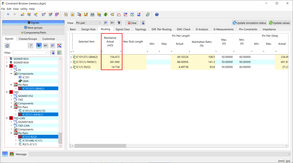
Alternatively, the solver can populate resistance values in the Constraint Browser for track substructures (so-called “pin-pairs”), allowing validation against resistance constraints, for example in power delivery networks with defined voltage drop limits.
Summary and Conclusion
Whether dealing with impedance or resistance during PCB design, Zuken CR-8000 provides designers with the capability to determine and control these electrical properties within its integrated PCB design and analysis environment.
Layout engineers are equipped to design a wide range of applications—from high-speed systems with tight impedance requirements to high-power designs such as battery management systems (BMS), where accurate control of current paths and load balancing is critical.
Additionally, dedicated tools for Signal Integrity (including transient simulation and S-parameter analysis) and Power Integrity (PDN analysis for AC/plane impedance and DC/IR-Drop effects) complement the CR-8000 platform for analysis-driven hardware development.

Ralf works as Product Manager for High-speed Design Systems at the Zuken EMC Technology Center in Paderborn/Germany, responsible for product marketing and business development for the Zuken SI, PI and EMC analysis tools. He holds a diploma degree in computer science, electrical engineering and economics from the University of Paderborn. He has 30 years of experience in Electronics and EDA. He is regular speaker on international conferences, but is involved in European Funding project and standardization activities as well.

- Blog
September 15, 2025
Signal Integrity Unplugged: Practical Ways to Make High-Speed Links Work (Podcast + Tips)
PCB Design, CR-8000, High-speed PCB Design, IBIS-AMI, PCB design, Signal Integrity

- Blog
May 23, 2025
AI in PCB Design: From Misconception to Meaningful Assistance
AI in PCB design is increasingly seen as a game-changer, with some predicting it could soon replace entire layout teams—but this view risks overlooking both the current limits of AI and the critical expertise engineering demands. At DesignCon 2025, experts from emphasized that AI's real value lies in complementing human judgment, not replacing it. Read more on our blog.
Read now

- Blog
February 13, 2025
The Future of Augmented Reality
Our new post explores the potential of augmented reality (AR) to transform everyday experiences in shopping, education, and navigation. It highlights how enhanced AR devices will offer immersive, interactive environments that blend the virtual and physical worlds.
Read now

- Blog
January 30, 2025
The Top PCB Design Trends to Watch in 2025
The field of PCB design continues to evolve as advancements in technology and shifting market demands push the boundaries of what’s possible. By 2025, several key trends are set to shape the industry. Find out more on our blog.
Read now