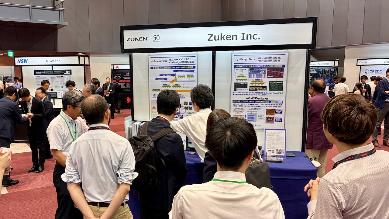
Zuken Joins TSMC’s Open Innovation Platform® EDA Alliance
WESTFORD, Mass., July 8, 2026 — Zuken Inc. today announced that it has joined the EDA Alliance in TSMC’s Open Innovation Platform® (OIP).
TSMC collaborates with its OIP EDA Alliance partners to address growing design demands, accelerate adoption of latest process and packaging technologies, and enable customers to achieve their PPA and time-to market targets. By participating in this alliance, Zuken will further enhance its IC packaging and printed circuit board (PCB) design products with the capabilities essential to support multi-die and chiplet-based designs using TSMC’s industry-leading technologies.
“We are pleased to welcome Zuken to the OIP EDA Alliance,” said Aveek Sarkar, Director of the Ecosystem and Alliance Management Division at TSMC. “The pursuit of higher performance and greater power efficiency continues to accelerate innovation in process and packaging technologies. By collaborating closely with EDA partners like Zuken, we enable customers to leverage TSMC’s advanced technologies to meet the demanding design targets of next-generation AI, HPC, and mobile applications.”
“By joining TSMC’s OIP EDA Alliance, Zuken will align its solutions with TSMC’s leading process and advanced packaging technologies. We are committed to helping our mutual customers seamlessly integrate semiconductor, package, and PCB design to meet today’s stringent system requirements,” said Ryosuke Takagi, Executive Officer and General Manager of the R&D Division at Zuken.
Related Resources

- Products
- Products
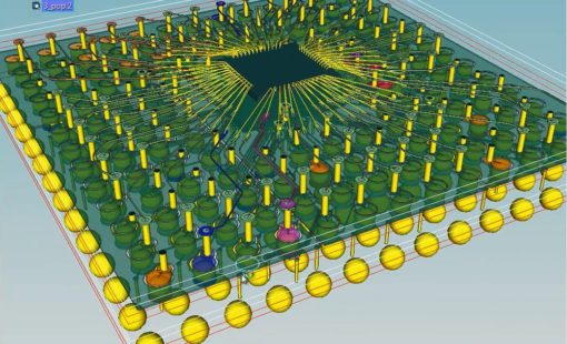
Design Force offers an intuitive, integrated environment for designing single and multi-die packages for wire-bond, flip-chip, and high density advanced packaging. Designers can start designs with early prototype input of chip and package data from the library, reuse data from IC layout tools, and take advantage of parametric wizards to streamline the creation of the system
- Products

- Products
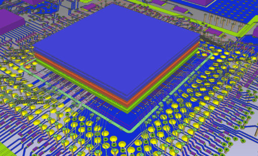
Building a competitive product today is much more difficult than a few years ago. Existing PCB-centric design processes are limited to a single PCB and do not provide the necessary tools for today’s competitive product development environment. PCB-centric design processes are falling behind.