Toshiba

achieves significant product size reduction using 3D chip, package, board co-design in CR-8000 Design Force

Toshiba faced a difficult design problem: their TransferJet™ technology was embedded in a customer cell phone, and when the next rev of the phone came around, they learned that they needed to shrink the board from 8mm x 8mm to 4.5mm x 6mm, and they had to shrink the module thickness from 1.7mm to 1.0mm.

The original design was a simple board with a wire bond package and several peripherals. Competitive pressures required a significant reduction in size and thickness. On top of that, they had to add RF matching to simplify the adoption of the module. Toshiba used Zuken’s CR-8000 Design Force with ANSYS analysis tools to accomplish the project.

Results

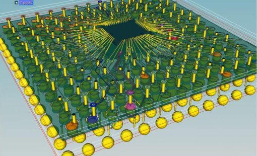
Reduction of board and module size was achieved by combining chip, package, and board into a 3D design structure for co-design feasibility studies.

Zuken’s CR-8000 Design Force enabled engineers to easily and quickly switch design context as they proceeded through the design process. When they needed to design the package in 3D, a click of a button switched to 3D mode, with another click, they were back in 2D, and with another click of a button they could design in the IC.

Easy location and correction of design issues due to tight coupling between CR-8000 and ANSYS analysis tools.

CR-8000 Design Force is the only tool that can tightly integrate semiconductor, package, and PCB devices, and provide the tight links to ANSYS tools for quick and accurate analysis results.

RF matching simplified adoption of the new module.

After analyzing dynamic noise, engineers found it exceeded their constraints. So from there, they built up a series of 30 possible solutions, and ran the analysis on each while applying a stimulus at the source of the noise on the IC. The software was able to identify the solution that gave the best results, reducing noise to 1/30th of the original measurement.

Feasibility studies took advantage of the 3D design and embedded design functionality in CR-8000 Design Force. They embedded the die and explored putting it face up and face down and also explored the effects of adding test pins. The die had the extra test pins, it was placed face down, embedded within the substrate, and employed ultra-thin shield coating on the package and an ultra-thin IC component.

How Toshiba used CR-8000 Design Force to solve their design problem

Play 0:56

toshiba-case-study-slides-300x211RF Module Shrink (TransferJetTM)

These slides are an abridgement of two presentations given by Toshiba at the Zuken Innovation World (ZIW) conference held in Japan in 2012 and 2013.

Download supporting slides

Download the full case study
 
Download supporting slides
 
Visit the Toshiba website

Discuss your design issues with our experts

We can help you craft the best solution for your company’s specific requirements
Get in touch