Mastering the Challenges of Modern PCB Design: Navigating Complexity, Cost, and Integration
The Evolution of Modern PCB Design Challenges
Printed Circuit Board design has been at the core of electronic innovation for decades. However, as technology advances, modern PCB design faces new challenges that make it increasingly complex and demanding.
In an era where electronic products continually evolve to be more feature-rich, smaller, and efficient, design engineers face the daunting task of achieving higher performance while minimizing costs. This balancing act necessitates careful component selection and optimization of routing to reduce signal losses. Additionally, it involves struggling with the increasing power demands of modern ICs, incorporating more power-integrity rules, and considering manufacturing processes to maximize yield without compromising quality.
Rising Complexity and Quantity of PCB Constraints Over Time
As the functionality of electronic devices increases, the fundamental laws of physics are still in place, imposing strict limitations. These laws govern how the signals on the boards propagate, interact, and dissipate heat within the circuitry. The miniaturization of components and the desire to cram more functionality into smaller form factors lead to increased design rules and constraints.
Modern memory capabilities, such as DDR4 and its low-power versions (e.g., LPDDR4), have become crucial across all industries. Operating at exceptionally high speeds requires careful consideration to ensure data signals reach the memory controller properly. This effectively sidesteps potential timing challenges that might otherwise result in data corruption or loss.
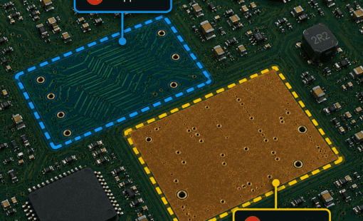
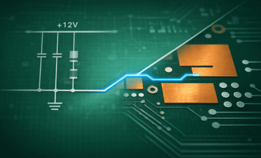
Among other factors, splitting planes or splitting plane cuts to distribute multiple voltages on the same PCB layer can drive complexity. However, this approach gives rise to irregularly shaped structures that can lead to the emergence of parasitic effects and resonances, significantly impacting power integrity and emissions.
As data transmission speed accelerates with USB, HDMI, or PCI express technology, amongst other things, signal integrity becomes a paramount concern. This necessitates meticulous attention to impedance matching, parasitic transmission line effects (e.g., losses, material roughness impact), and crosstalk mitigation. The foundation of such data transmission standards is differential protocols, which allow the transmission of high-speed data streams through differential pairs. Moreover, differential pairs may take up twice as much space on a PCB. Still, they generate minimal interference and are more immune to ground discontinuities and noise effects than other types.
Key Guidelines in High-Speed Design
Meeting the design rules and constraints imposed by these technological advancements is essential to achieve a functioning product that meets the required performance, reliability, and manufacturability standards.
The most common design rules in high-speed, modern PCB design include:
- Length matching rules for differential pairs
- Traces crossing split planes, return current potentially guided by stitching capacitors
- Rules controlling the maximum allowed length for stubs (short trace segments to connect ICs or test-points
- Routing of signals in parallel
- The impact of length differences within complex ICs and the necessity to compensate that on the board (if not using flip-chip technology)
The Importance of Virtual Prototyping in Modern PCB Design
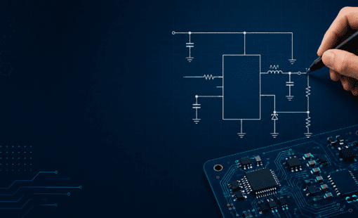
A powerful tool to navigate the new challenges of modern PCB design is the use of virtual prototyping. With the rapid pace of technological advancements, waiting for physical prototypes to identify issues can be time-consuming and costly. Therefore, virtual prototyping enables designers to simulate and validate their designs in a virtual environment. This allows them to make qualified design decisions before committing to physical (mass) manufacturing.
As a result, early detection of potential signal and power integrity problems, thermal issues, and other design pitfalls can be identified. By harnessing sophisticated software, engineers can assess various scenarios and optimize component placement within a digital realm. They can also fine-tune routing strategies in this virtual environment. This expedites the design process and significantly reduces the likelihood of costly errors.
Zuken’s CR-8000 provides a comprehensive platform for simulating and analyzing modern PCB designs with embedded power and signal integrity analysis and electromagnetic interference checks. Whether you are working on a single-board or multi-board project, this software provides a complete set of tools to maintain the integrity and reliability of your PCB designs.
Conclusion
Modern PCB design today is undoubtedly more challenging than it used to be. As electronic devices become more capable, the laws of physics remain steadfast, imposing rigorous limitations. These limitations affect signal propagation, heat dissipation, and component interaction. Mastering the intricate dance between complexity, cost considerations, and integration is essential for creating electronic marvels that power our lives. Tools that enable constraint management and the simulation of different scenarios help navigate the landscape of modern PCB design.

-
Product Manager/Senior Consultant

- Blog
- Blog
- Blog
- Blog
Related Products and Resources

- Webinar
- Webinar
- Products
Building a competitive product today is much more difficult than a few years ago. Existing PCB-centric design processes are limited to a single PCB and do not provide the necessary tools for today’s competitive product development environment. PCB-centric design processes are falling behind.