Programmable Logic
Unified FPGA and PCB design
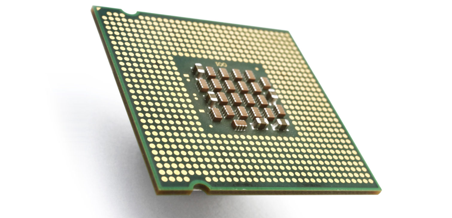
FPGAs are replacing ASICs in many design applications. They are also used for prototyping designs, implementing ASICs, or other embedded hardware and software design, as they can easily be reprogrammed. Engineering teams require an effective design flow, unifying FPGA and PCB design to reduce design cycle times and improve time-to-market.

We can help you with
-
Concurrent design of FPGAs and PCBs
-
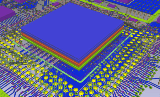
An effective FPGA/PCB co-design environment, providing support for the latest devices offered by FPGA vendors. As part of Zuken’s system level design suite, our solution enables design teams to intelligently communicate pin I/O assignment information on FPGAs or other high pin count devices with our Design Gateway and Design Force PCB design tools.
-
System Level Circuit Engineering
-
True system-level circuit design in which individual circuits can be represented and connected as blocks. This approach enables engineers to manage signal continuity (interconnects) at the system level rather than just at the design level, allowing for an evaluation of board-to-board signal continuity.
-
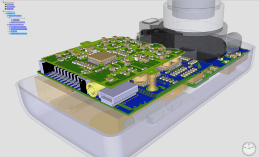
3D Multi-board PCB Design
-
A complete environment to manage the design of FPGAs, ASICs and other high-pin count devices on a PCB. As the initial FPGA is simulated and synthesized, engineers can load the logical and physical circuit design to review pin assignments and constraint.
Related products

- Products
Graphical Pin Manager offers an effective FPGA / PCB co-design environment providing support for the latest devices offered by FPGA vendors

- Products
CR-8000 Design Gateway provides a platform for logical circuit design and verification of multi-board system-level electronic designs.
- Products
CR-8000 Design Force is the fastest, most effective PCB design solution available today. Design Force enables design teams to layout and verify their designs in the context of a complete system or product.
More on FPGA Co-design solutions
Check our latest webinars, white papers, blog posts and more
- Webinar
- White Paper

- Press Release