Tech Tip: Using Design Force Rule Editor to Calculate Track Impedance
Today are going to discuss how to use Design Force rule editor to calculate track impedance.
Calculate the track width value from the characteristic impedance and layer configuration by using a field solver.
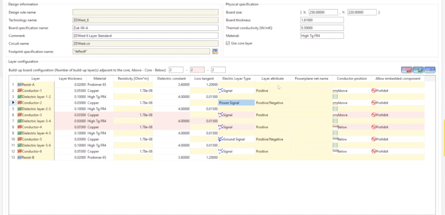
In [Layer Configuration] on the [Board Configuration] tab, set the thickness, resistivity, dielectric constant, and loss tangent values for all the layers.
Also, set the reference plane layer that matches the following conditions
A layer with the Layer attribute set to Power Plane is handled as a reference layer. If there is no Power Plane layer, a layer with the Electric layer type set to Power or Ground is handled as a reference plane. (The electric layer type of power or ground must be set for two or more layers.)
If the layer to be calculated is a power or ground layer, the power or ground layer located closest (upward or downward) to that layer is handled as a reference layer.
Click the [Calculate Char. Z -> Track Width] button in the upper part of the [Track width stack] table to open the dialog.
From the track width stack list, select the track width stack.
Set [Target Char. Z].
Set the [Rounding precision for track width] value
Calculate the track width value using a field solver until the specified rounding precision is reached.
Click the [Calculate Track Width] button. The calculation result is displayed in the [Track width] cell.
The range of track width that can be calculated is between 0.00001 mm and 5 mm.
Click the [Apply calculated results to track width stack] button to apply the track width value obtained from the calculation to the track width rule stack.
Differential Pairs are handled a little differently.
Click the [Calculate Diff. Z -> Track Width] button in the upper part of the [Differential pair rule stack] table to open the dialog.
From the track width stack list, select the differential pair rule stack.
Select [Calculation mode].
- Calculating track width from differential Z and track spacing
- Select [Track width] from [Calculation mode], and specify [Target Diff. Z] and [Track spacing].
- Calculating track spacing from differential Z and track width
- Select [Track spacing] from [Calculation mode] and specify [Target Diff. Z] and [Track width].
Set the [Rounding precision for track width (spacing)] value
Calculate the track width and spacing values using a field solver until the specified rounding precision is reached.
Click the [Calculate Track Width (Spacing)] button. The calculation result is displayed in the target cell (track width or spacing).
The range of track width and spacing that can be calculated is between 0.00001 mm and 5 mm.
Click the [Apply calculated results to diff. rule stack] button to apply the track width and spacing values obtained from the calculation to the differential pair rule stack.

-
Applications Engineer


- Blog

- Blog

- Blog

- Blog
Related Products and Resources

- Products
Design Force offers an intuitive, integrated environment for designing single and multi-die packages for wire-bond, flip-chip, and high density advanced packaging. Designers can start designs with early prototype input of chip and package data from the library, reuse data from IC layout tools, and take advantage of parametric wizards to streamline the creation of the system

- Products
Design Force combines traditional 2D design with native 3D design and the latest human interface techniques, accelerated graphics and almost instantaneous rendering and refreshing. It is the fastest, most effective PCB design solution available today. Design Force enables design teams to layout their designs in the context of a complete system or product.

- Products
Building a competitive product today is much more difficult than a few years ago. Existing PCB-centric design processes are limited to a single PCB and do not provide the necessary tools for today’s competitive product development environment. PCB-centric design processes are falling behind.