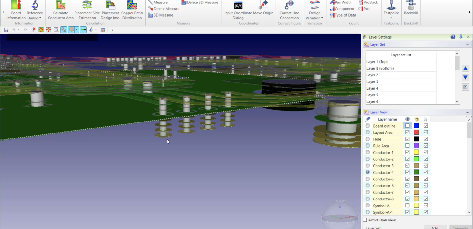
Tech Tip: How to Generate Back Drill Data and Obstacles in a PCB Design
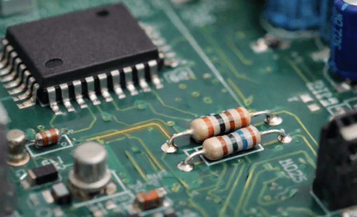
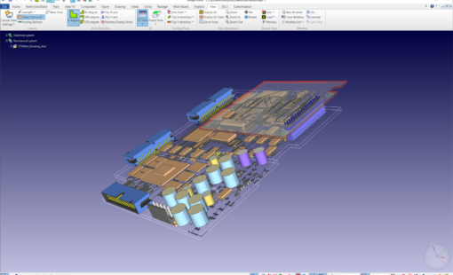
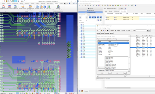
PCB backdrilling has been used for years as a means of removing excess parasitic effects from via stubs. This is done by drilling an oversized hole into a via, thus cutting away the excess metal. This process is mostly used when high speed switching is used and simulation results warrant the removal of the via stub. CR-8000 Design Force supports a new dynamic method of preparing a PCB for backdrilling. This is supported at the net level and by the layer spans. The process automatically creates track and via keep outs around the holes that will be oversized.
Check out the two-part video series that demonstrates this process.
Part 1: Preparing for backdrilling
Part 2: Generating the data output

-
Applications Engineer

- Blog
- Blog
- Blog
- Blog
Related Products & Resources

- Blog
- Press Release
CR-8000 from Zuken advances system-level PCB design with significant enhancements in analog simulation, SI analysis, and intelligent layout and routing
- Blog

- Products
Building a competitive product today is much more difficult than a few years ago. Existing PCB-centric design processes are limited to a single PCB and do not provide the necessary tools for today’s competitive product development environment. PCB-centric design processes are falling behind.