Tech Tip: Creating a Cavity in a PCB Design using CR-8000 Design Force
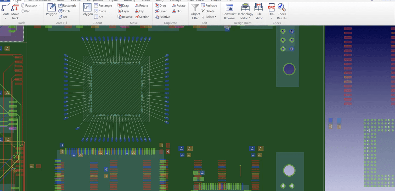
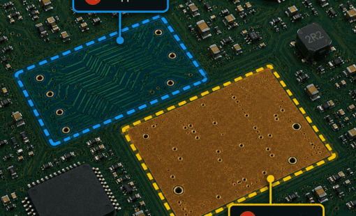
A Cavity is a cutout in the PCB going from the outer copper layer to an inner copper layer, but not totally through the PCB. The use of cavities in a PCB is a method to reduce the component height or to increase component clearances. It also can be used for real estate constraints and heat requirements, to name a few. A Cavity is created on the fly, inside Design Force, or built into the footprint at the library level. A Technology for Inner Component Design is necessary. Footprints are also to be created for inner layers.
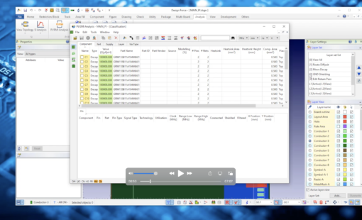
The following video will demonstrate creating a cavity.

-
Applications Engineer

- Blog

- Blog
- Blog

- Blog
Related Products & Resources
- Blog
- Blog

- Software Viewer

- Products
Building a competitive product today is much more difficult than a few years ago. Existing PCB-centric design processes are limited to a single PCB and do not provide the necessary tools for today’s competitive product development environment. PCB-centric design processes are falling behind.