
IoT Makes Complex Design Problems Mass Market – Part 2
In the first part of this blog series (here), I looked at the explosion in the growth of internet connected technology and wearable devices, and started to look at what kind of design challenges this posed; not just for cutting edge niche products, but mass market general electronics goods.
I started to explore the need to collaborate on a mechanical level; but the level of integration really needed to compete in this space goes far beyond that.
Cross-discipline collaboration
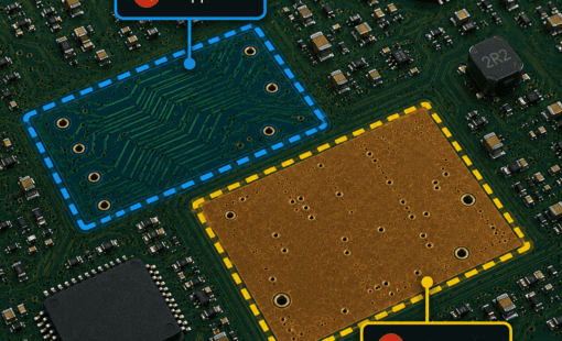
This shouldn’t be limited to PCB and mechanical disciplines – there’s a need for collaboration across the system. Traditionally, the PCB, package, IC and enclosures are each designed in their own stand-alone 2D environment. With increasing functionality, tight schedules, tighter cost constraints, and the decreasing form factor of today’s IoT and wearable products, components need to be tightly coordinated with one another so that pin assignments can be optimized for small size and minimum layer count substrates. The overall goal is to align the boards, packages and chips so that signals follow the shortest possible path in the fewest layers possible from the chip through the board to the chip, resulting in the fewest possible layers across all substrates.

Managing complex 2.5/3D package interconnect with TSVs
It’s important now to be integrating detailed design using PCBs, packages and ICs, within their mechanical enclosure.
- Viewing the IC, package and PCB simultaneously allows you to optimize pin assignments faster and more accurately.
- You can perform system-level optimization, detailed package, PCB, and interposer design, while optimizing the IC RDL routing, die bump placement and power mesh in a single cockpit.
- Then there’s optimization of different package layers while considering the routing on the redistribution layer (RDL) and placement on the IC side and the escape route on the PCB side in a single design view.
With this in mind, we’ve made it so that our 3D, multi-design environment enables a true view of the routing interdependencies of complex packages so you can do all the things I’m preaching about above.
Concurrent engineering and design with multi-physics, multi-discipline simulation and analysis
Here’s some other areas of design collaboration that are going to make you more competitive and reduce risk:
-

Concurrently verify signal performance with integrated signal and power integrity analysis during product design
Multiple IC importing connected together using industry standards (GDS or LEF/DEF) and hosting in OpenAccess database format.
- Multi-discipline, multi-physics analysis with integrated signal integrity, power integrity and electromagnetic interference analysis.
- Design reuse by using blocks, reusing elements like schematics, parts lists and layout elements with controlled user access.
- Multi-board and native 3D design

CR-8000 is our integrated 3D multi-board chip/package/board co-design environment that makes it possible to holistically optimize the package, board and IC design to a greater degree than was possible in the past, with the end result being higher performance and lower manufacturing costs. On a system-level aspect it allows engineers to quickly explore the design space while considering the effects of alternate approaches on functionality, price, performance, size weight and style.
- Blog

- Blog
- Blog

- Blog
Related Products and Resources

- Products

- Products
Zuken’s engineering data management platform DS-CR has been created to support the specific demands of PCB design data management. It combines multi-site library, design data and configuration management into a unified engineering environment.

- Products
Building a competitive product today is much more difficult than a few years ago. Existing PCB-centric design processes are limited to a single PCB and do not provide the necessary tools for today’s competitive product development environment. PCB-centric design processes are falling behind.