
Inside Signal Integrity: Impedance Control – Part 2
In part 1 of this blog we took a back-to-basics approach and discussed line impedance and its effects in signal integrity. As every electrical conductor comprises capacitance, an inductance, and a frequency-dependent ohmic resistance, and with increasing frequencies, these electrical characteristics will influence and distort the signal.
Applying a transmission line model based on the telegrapher’s equations (as typically common in signal integrity considerations except for when considering extremely high data rates, e.g., SERDES channels), one often used the general expression for the characteristic impedance of a lossy transmission line is:
where:
R = the resistance per unit length, considering the two conductors to be in series,
L = the inductance per unit length,
G = the conductance of the dielectric per unit length,
C = the capacitance per unit length,
j = the imaginary unit, and
w = is the angular frequency
As for the transmission line model, it was shown in part 1 of this blog but is worth showing again here as a reminder (see figure 1).

Figure 1: Equivalent circuit of a transmission line (Source: Wikipedia)
Although an infinite line is assumed, the characteristic impedance is independent of the length of the transmission line (as all quantities are per unit length). Hence, the electrical behavior of a digital signal is mainly determined by the geometry of the conductor. It is, therefore, possible to compute the above parameters and derive impedance and signal velocities from them. NB: the material characteristics of the insulator material (=dielectrics) must also be known.
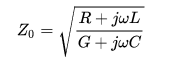
If a certain impedance is to be achieved for given track dimensions (as specified by the PCB manufacturer), then by varying the dielectric height it is possible to achieve the required impedance value (see figure 2). Alternatively, the developer may also vary the dielectric material and thus influence the impedance by controlling the L and C characteristics. NB: for simplification, we are considering a lossless case; i.e., we neglect the frequency-dependent parameters R and G for the moment and assume that there is no line resistance and no dielectric loss.
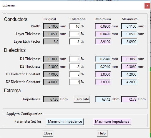
Figure 2: Varying the dielectric properties can help you achieve the desired track impedance (Zuken Field Solver GUI)
As the dielectric constant er primarily influences the propagation of the E and H fields and the current flow through the conductor, it is obvious how important the surrounding medium (the dielectric material) is on the achieved impedance and the signal propagation.
If there is no signal reference (ground or supply layer) in the immediate vicinity of the signal line, the signal return path is somewhat variable and the impedance value of the transmission line can get very high. Worst case it can get close to that of a single line in air (ZL = approximately 377W).
Due to the varying input resistances and the different switching behavior of the ICs on a board, various impedance targets need to be matched when designing a large PCB. This makes it crucial for the developer to know about the design constraints resulting from the layer stack structure (see figure 3) during the design process.
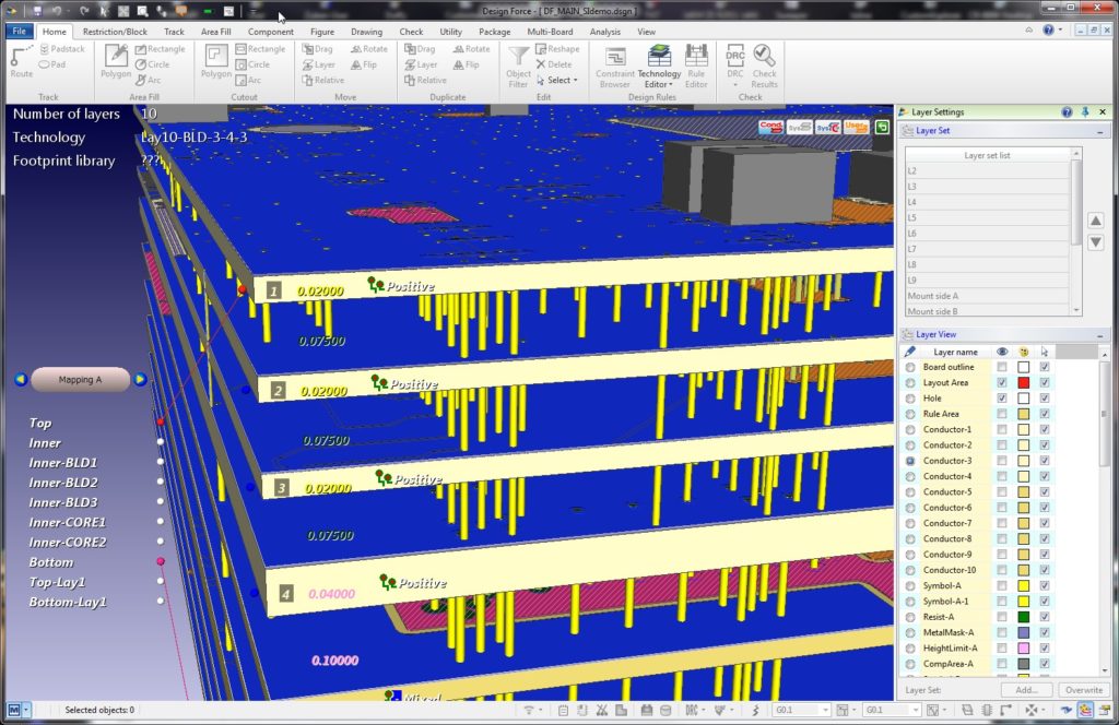
Figure 3: An example layer-stack structure (3D image captured in Zuken’s CR-8000 Design Force).
Common engineering practice is to build, over time, a library of known layer-stacks with defined impedance configurations, so that developers can relate to set values and not have to develop a new layer structure every time.
Visualizing the structure in 2D (or in 3D) helps to takes the pain out of handling increasing design complexity. NB: in particularly challenging high-speed designs, it is a common (but costly) practice to order impedance-controlled printed circuit boards – as all the design constraints and calculations were made during the design. Also, please note, that impedance-controlled PCBs are not produced using higher accuracy processes; as the ‘control’ implies the creation of test coupons for all possible impedance situations on all layers and enhanced testing whether the target is met or not. Proper impedance planning early in the design phase can help save the (typically) 25% premium you’ll pay for impedance-controlled boards.
The calculation of impedances (especially when done by the formulas employed by web-based design tools) usually takes the assumption of a rectangular cross-section of the finished circuit trace with a perfect current return path. However, the real cross-section is more likely to be a polygon approaching a trapezoidal shape; sometimes crosses gaps in the reference layer underneath (current return) and can vary widely from board manufacturer to board manufacturer.
This then raises the question whether the assumption of a rectangular cross-section for an impedance calculation is accurate enough – and will signal integrity to be compromised by this non-perfectly-shaped cross-section? The field solver can take into account the etching changing the trace geometry, and they can detect situations where the track shows a so-called discontinuity as well.
As mentioned in part 1 of this blog, to ensure a reflection-free signal, high-speed nets require impedance matching. This means that the driver (output resistance), the transmission line and the receiver must show as little as possible (and ideally no) impedance difference values. In contrast, unmatched signals then show significant distortion as shown in figure 4.
Figure 4: Signal integrity – terminated signal matching the impedance (right) vs. unmatched (left)
However, routing may cause other issues. For instance, branches in topologies (see Figure 5) can create a voltage divider and produce therefore a reflection point – despite a supposed ideal adaptation of the same resistance in all legs (perfect matching requires we use Kirchhoff’s law for resistance in parallel).
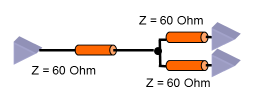
Figure 5: A branched topology.
Do you need to be 100% on target? Yes and No
In digital electronics, data and information are often exchanged point-to-point between two components. It is mandatory, that information is transmitted without being distorted or delayed.
It can be concluded that the signal integrity of critical signals must be ensured; hence, impedance control is the first step to do so. The decision of whether a signal still arrives with sufficient quality must be answered on the basis of the circuit characteristics and the component specifications. In many cases, components can detect the switching information even if the signal is slightly distorted. Alternatively, modern silicon can be programmed via hardware settings to significantly improve the signal quality at the receiver. If available, this option should always be used when working ‘close to the limits’ with regard to signal integrity budgets. Alternatives can be explored through signal integrity simulations.
To judge the effect on the signals, you must consider the two major reasons for impedance matching:
- Control the delay
- Reduce reflections and attenuation.
In the fan-out area of high-pin BGAs, traces are often ‘necked-down’ for routing space reasons between the BGA balls, which creates an impedance mismatch (i.e., a reflection situation). A typical 50Ω trace on an inner layer has a propagation delay of about 6 ns per m. If this transmission line is part of a differential pair and traverses (for instance) a BGA breakout region and has a ±30% impedance mismatch (i.e. 65Ω) over a length of 3 cm, the signal transit time will be delayed by 6ps. This will create a small phase shift even at 3GHz. Not too much of a concern. The bigger the issue is the risk of reflections.
Often, an exact adaptation of the impedance is not possible (and often unnecessary). Smaller mismatches are often still acceptable, as the proper logical switching of the signals is ensured by the semiconductors’ switching tolerances.
However, no general design rule should be inferred from this. In such cases, it is more important to minimize the deviations of the impedances – and of course to be aware of the consequences. SI simulations tools like the CR-8000 Analysis Module will reveal their virtual prototyping power in such situations.
An example of the real-life impact of matched impedance is shown in figure 6, where the switching behavior of a DDR3 data signal (point-to-point, the receiver only) is shown and where the memory vendor (Micron) demanded an impedance value of 50Ω.
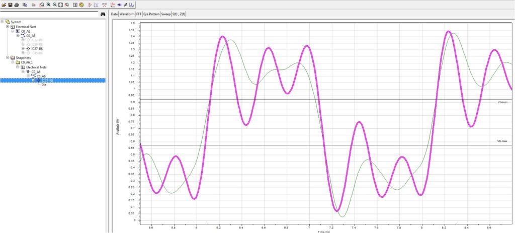
Figure 6: DDR3 Data Signal with 60Ω (magenta) and 42Ω (green)
During the final verification of the PCB, the designer controlled all traces of the DDR3 interface using the Zuken SI simulator, considering all possible manufacturing tolerances (20% was stated by the board manufacturer). When reaching the upper tolerance boundary of 60Ω, proper switching could not be ensured (a serious ring-back below the threshold is visible, yielding a timing error) whereas, closer to the lower boundary (between 42 and 45Ω) signal behavior is best.
This shows the strength of concurrent simulation as part of the design process and the benefits of conducting investigations on the virtual prototype.
Conclusion
For the cost-effective development of high-speed printed circuit boards, it is important to not only know the different options of impedance-controlled design but also to know (or define) the necessary and achievable tolerances.
A proven approach is to constrain up-front, design to target impedances and to optimize the PCB. The effects of an impedance mismatch must be known and understood and, in this respect, the use of simulation tools and virtual prototyping is key to success. In addition, close collaboration with the PCB manufacturer – during the early stages of your project – is highly recommended. Indeed, the CAM departments of your PCB manufacturer can often provide proper indications to solve all impedance-related design questions. However, designers are advised not to hand over the control of impedance issues to external parties.
Learn more


- Blog

- Blog

- Blog

- Blog