Tips for Running Successful SI Simulations
If you’re anything like me, you love that feeling when your simulations match your measurements and calculations. It’s one of those special treats that only engineers recognize. Drawing such a close line between theory and reality is tough. Many things must be set up just right to get that level of correlation. In the world of SI simulations, three main things must be just right: the model selection, the stimulus setup, and the board setup. We’ll take a closer look at how those elements can set you up for running successful SI simulations.
IBIS Model and SI Simulation
IBIS Model Basics
Let’s level-set a little bit and spend a few minutes on what our driver and receiver models are built from–the IBIS model. IBIS models electrical behavior without exposing any proprietary internal structure of a device, which is perhaps one of the factors contributing to its success. These models are also ASCII-based and human-readable.
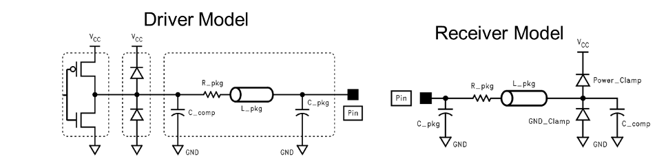
The IBIS model defines the characteristics of the driver and the receiver. The driver model consists of a CMOS inverter representing the output driver of an IC. The receiver model is a little more passive in a way; it consists of the receiver’s parasitic capacitance, resistance, and inductance. Either way, the inside of an IBIS model requires a clear definition of several things. In general terms, it consists of three main elements:
- The operating conditions and parameters of the device in question. This includes things like maximum and minimum voltages.
- The parasitics that arise from the traces and metal components of the package. This includes the package self-inductance, capacitance, and resistance, as well as other related non-idealities of that type.
- The model uses three primary tables to define the switching characteristics of the device: the IV curve of the active components in the device, time-dependent voltage, and current ramps.
The idea behind IBIS models is fairly simple and, likewise, fairly powerful and can be an asset when making plans for running successful SI simulations.
Know Your IBIS Model
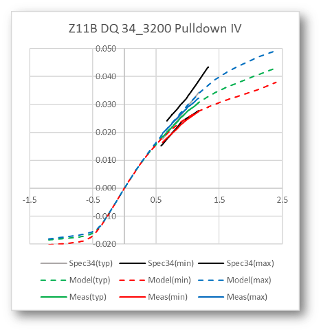
Figure 2 is an example of a model from Micron. We won’t always get this type of clarity from the vendor. However, it is easy to see that the more we move away from the linear portion of the model, the more error we see. It is not only important to know what you’re simulating but how and under which conditions you can expect the most accuracy. Generally, the closer you get to limits, the more you’ll deviate, so don’t forget to consider that in your simulation.
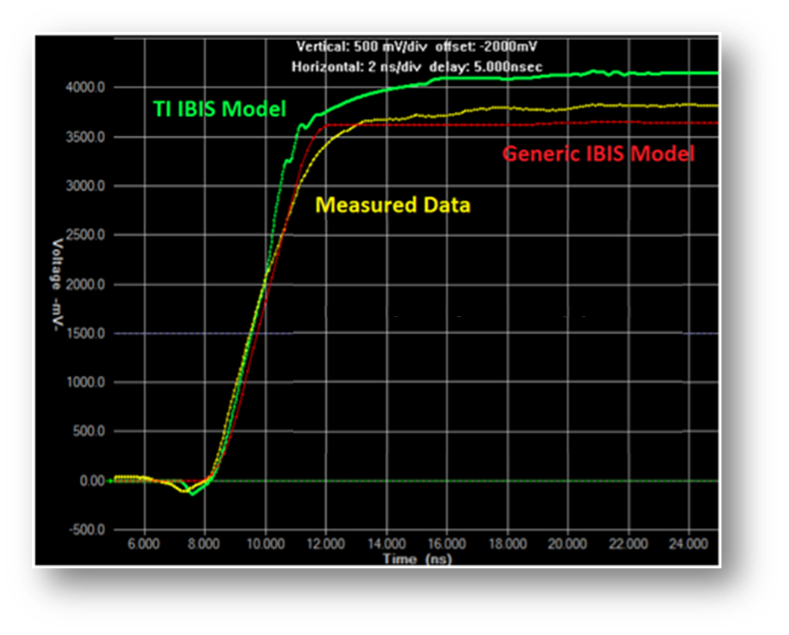
Figure 3 compares a real-world measurement, a generic IBIS model, and a vendor-supplied IBIS model. As you can see, the red line representing the generic IBIS model is almost an ideal curve with no undershoots or overshoots. The green vendor-supplied model is more sophisticated, including some higher-order effects. The yellow curve is measured data that seems to agree more with the vendor-supplied model. That’s not to say that the vendor-supplied model is the perfect way to go…
If you look closely, the rise time of the generic model actually agrees more with the measured data. So, it is essential to keep in mind what you’re looking for and what you’re simulating. The vendor model might be better if I’m looking for overshoots and undershoots. However, the generic model might produce a more accurate representation if I’m looking for eye width. Therefore, the more we know about our model, the more effective tool it can be. If you’re using a part that is produced by different suppliers, it is a good idea to simulate with models from all vendors and design to the worst case of those scenarios.
SI Simulations and Identifying the Best Stimulus
Choosing Data and Timing for an SI Simulation
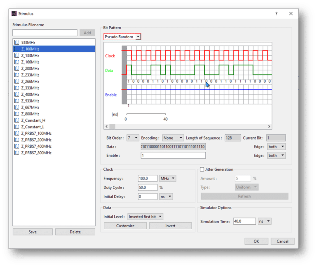
One part of the stimulus is the voltage and slew rate, which we will get to later when we discuss corner case selection. The other side of the stimulus coin is bit patterns and characteristics. When testing a clock signal, a periodic pulse train would give a good sense of what the overall signal integrity is likely to be and is representative of a real-world use case. When testing data signals, a pseudorandom bit sequence is a good representation of what your signal is likely to see. It is also a good data sequence for eye pattern and jitter analysis.
SI Drive Strengths
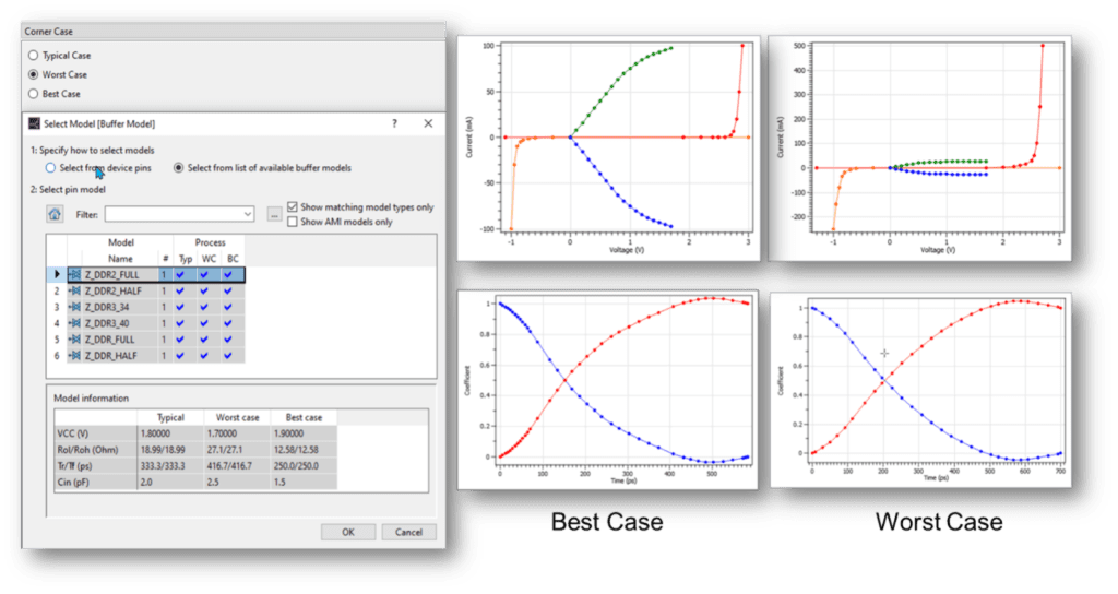
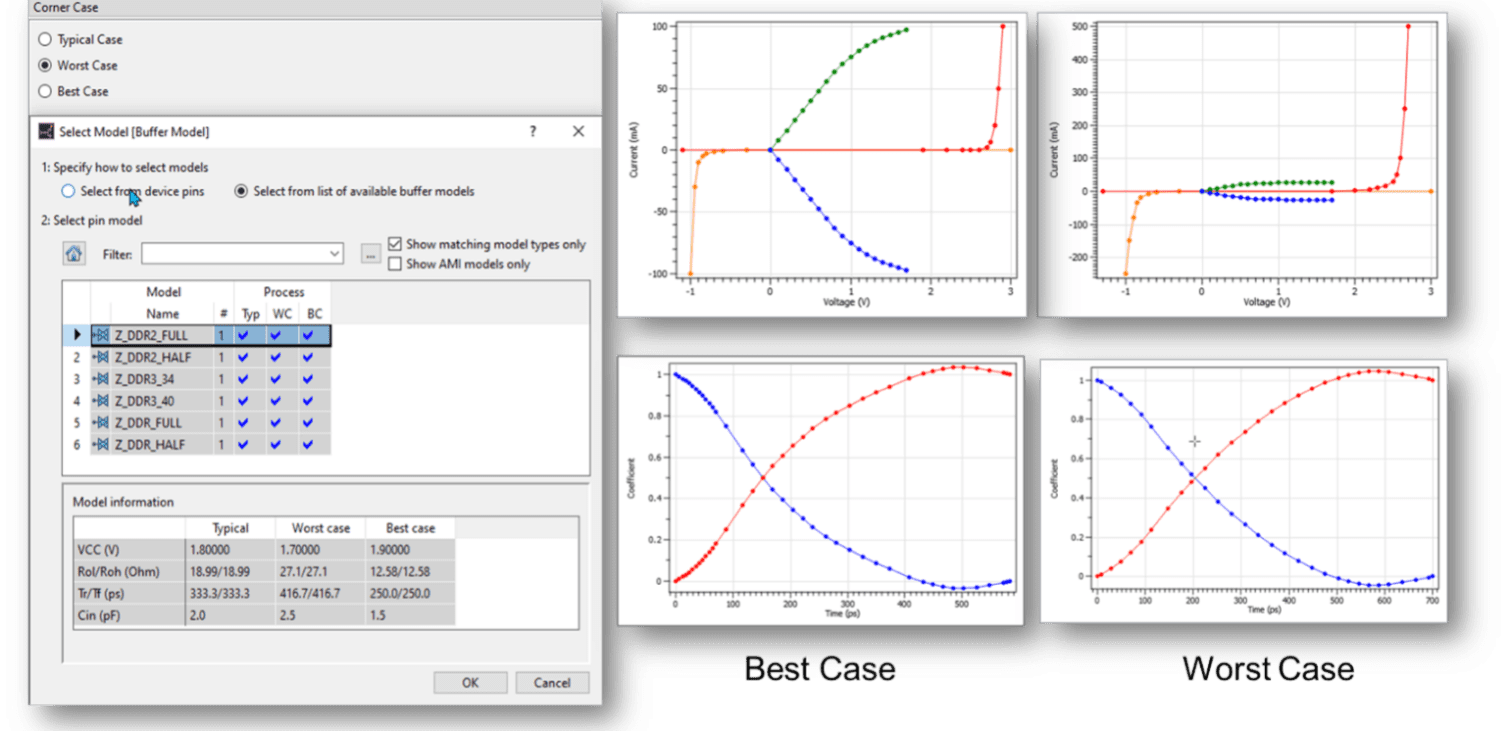
Correctly setting up the stimulus is an integral part of the SI journey. IBIS models can represent three different corner cases, and we can also draw similar inferences from drive strength selection:
- The typical scenario where all the voltages, rise/fall times, and parasitics are in their nominal values and at the center of the design targets.
- The worst-case scenario represents the low end of the operating parameters where voltages are lower than typical and have slower rise and fall times.
- The term best case scenario is misleading. It represents the upper end of the corner cases, where voltages are at or near their spec limit and rise and fall times are much faster.
Doing an SI simulation with the worst-case scenario will represent what happens in depressed conditions where speeds and power supplies are slightly slower. Using the so-called best-case scenario will bring to light any possible over or undershoots.
Setting up PCB Parameters for SI Simulations
The most significant contributor to signal integrity performance is the PCB itself. It is the transmission line through which signals pass. This is perhaps the setup that is most critical to get right.
PCB Stack-up Considerations
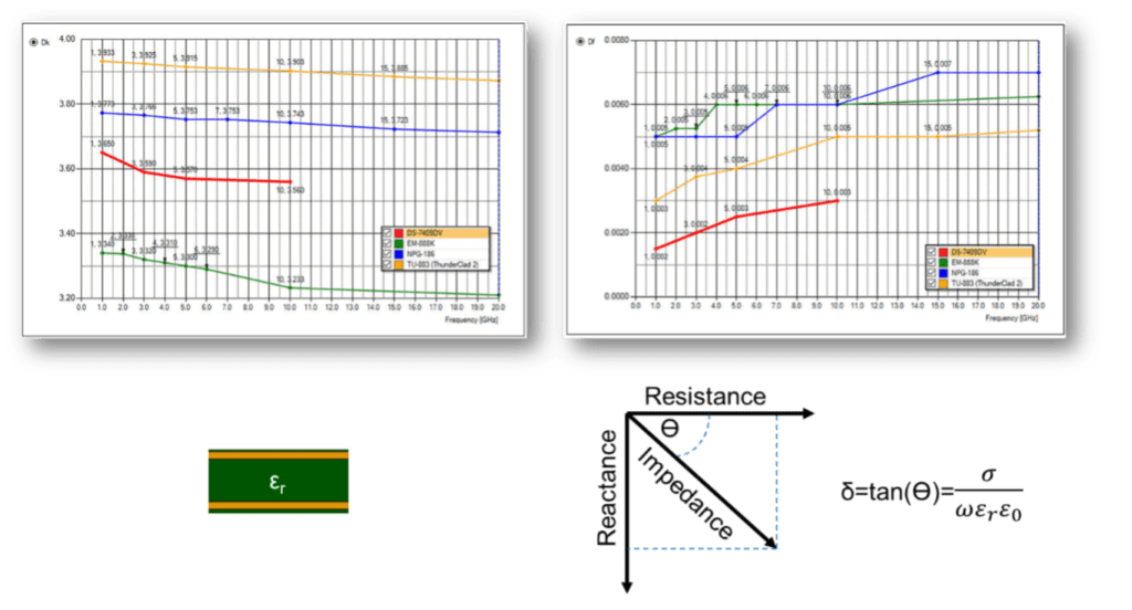
Two of the most important factors to keep in mind when selecting board materials are the dielectric constant and the dissipation factor, sometimes called the loss tangent.
The dielectric constant is the electrical isolation between board layers; the higher this number is, the more insulated signals on different layers are from one another. That comes with a caveat–increased layer-to-layer capacitance–so you have to strike a balance. Sometimes so-called “high-K” material can be more expensive, and if you don’t need the isolation, then it can be a bit of a waste. Either way, the dielectric constant is one of the first things we consider when selecting board materials.
The other quantity, the dissipation factor (DF), is closely related to the dielectric constant. Think of the dissipation factor as a measure of the ability to transmit power without reactive power losses. The lower this quantity is, the lower the imaginary loss to our signal, and believe it is real! High DF could cause heating and angular signal distortion and delay. For those with a keen eye, you’ll notice a critical element in the denominator of the DF equation. There is a frequency dependency. So, when simulating, it is important to know what the DF is at your particular target frequency, as it can vary a bit.
For the pedantic among us, the dielectric constant also varies with frequency, but it is a relatively flat curve with only a slight variation.
Accounting for All PCB Layers
Once you’ve made the material choice parameters, it is important to input those into the board stack-up editor. If you enter those figures incorrectly or make the wrong selection, then the signal integrity simulation will not be accurate. Even something as seemingly innocuous as the resist layer or the silk screen layer should be accounted for to ensure the most true-to-life simulation results.
PCB Manufacturing Effect Consideration
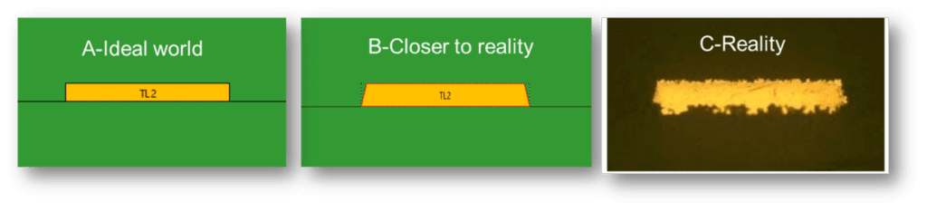
Advanced SI simulation tools also allow you to consider effects due to manufacturing. Wouldn’t it be great if all our etch lines and edges were perfectly sharp and idealized? Well, that’s not the case, and when copper traces are etched out, they are shaped more like trapezoids because the etching agent acts more on the top of the trace than the bottom, leaving the cross-section chamfered. Furthermore, the etching process leaves a rough surface on the copper. These effects might seem minimal, but when considering high-speed signals in the high hundreds of megahertz or even gigahertz, things like this matter considerably. Zuken’s simulation tools in the eCADSTAR or CR-8000 tool suites take these effects into account, leaving you with a clearer picture of signal integrity expectations.
Conclusion
Running successful SI simulations means that all the various knobs and variables that drive the simulation must be as accurate to the expected real-world performance as possible. It’s the typical garbage-in, garbage-out scenario. Spending more time on the front end of the setup results in less time making sense of or questioning the results. (Though we should always question results, and it becomes much easier with rigor in the setup). To see how setup affects simulation results, try an eCADSTAR test drive today by clicking this link: https://pages.zuken.com/eCADSTAR-Test-Drive.html.

- Blog

- Blog

- Blog

- Blog
Related Products & Resources
Additional Products and Resources