Tech Tips: Batch Selection of No Net Routing Patterns DF-2024
Menu
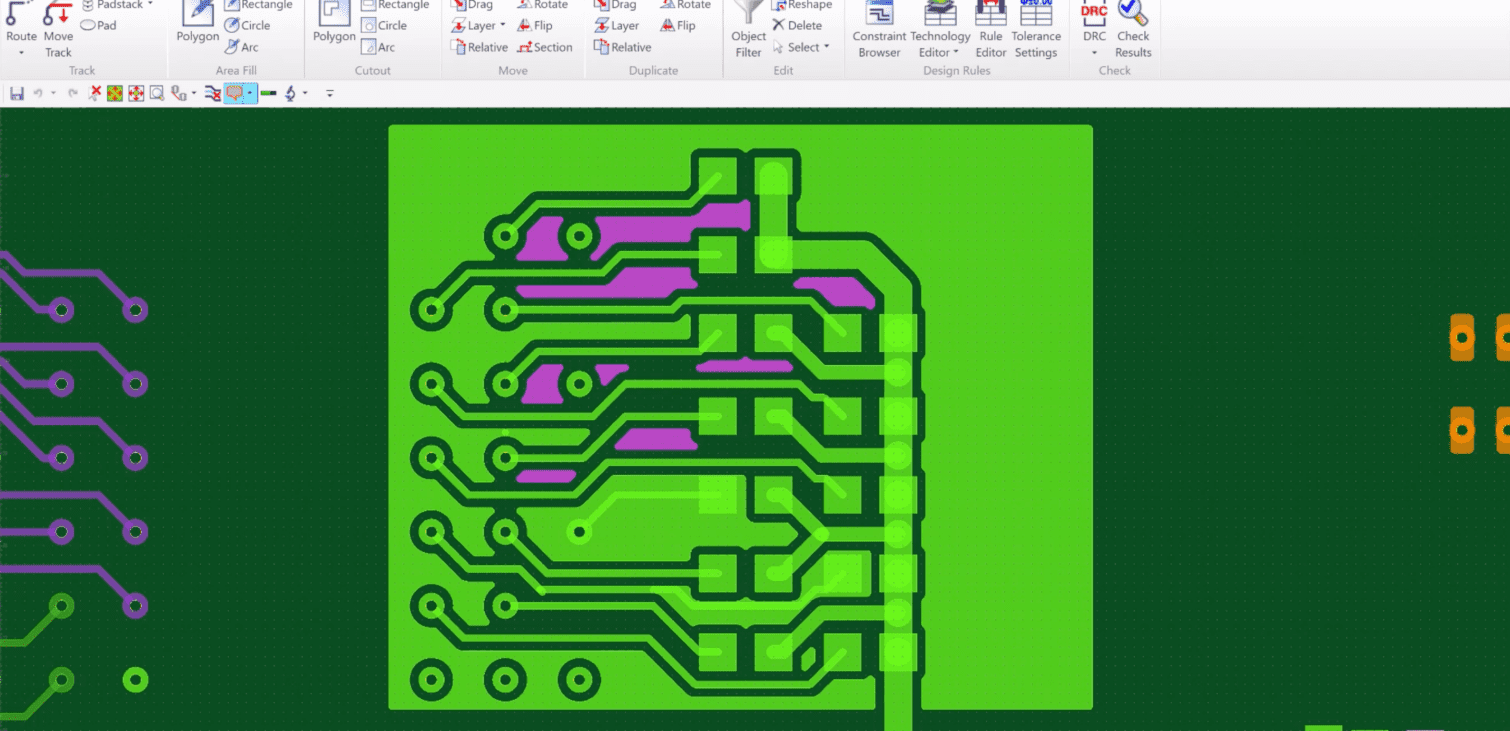
Streamlining the PCB Design Process
A new feature now allows PCB designers to select and delete all “No Net Routing Patterns” in a single operation, significantly speeding up the design cycle.
What Are “No Net Routing Patterns”?
A “No Net Routing Pattern” refers to excess copper that may be unintentionally left on a PCB during the design process. This often happens after multiple copper area fills. Additionally, tracks without an assigned net may remain due to schematic changes and Forward Annotation updates.
Why Remove Floating Copper?
Leaving floating copper in a PCB design can lead to electromagnetic compatibility (EMC) issues, especially at high frequencies. These unconnected copper sections can:
- Pick up noise from surrounding components
- Act as resonators, impacting circuit performance
- Cause excessive radiation, leading to compliance failures
Demonstration Video
The following video demonstrates how to efficiently remove “No Net Routing Patterns” using CR-8000 V2024.

-
Applications Engineer

Jeff Perry is a Customer Support Applications Engineer. He focuses on customer support for CR-5000/CR-8000 Tool Suites. Jeff provides instruction on Zuken tools at customer sites or via the web. He also puts together Application Notes, Tool Tips and Tech Tips which help improve customer productivity. He enjoys golf and spending time with his grandson.

- Blog
February 24, 2026
Tech Tip: Template Area Net Check Prevents Copper Net Mismatches
cr-8000, PCB Design, Tech-Tips, Blog
- Blog
February 19, 2026
Circuit Diagram Design: A Practical Guide for Modern Engineering Teams
cr-8000, Digital Engineering, e3-series, Electrical, Electrical & Wire Harness, Electronic, PCB Design, circuit diagrams, CR-8000, E3.series, Electrical Design, engineering documentation, PCB Tools, schematic design, wiring diagrams, Blog

- Blog
January 08, 2026
Top 10 Blog Posts of 2025
Americas, cr-8000, DS-E3, e3-series, Electrical & Wire Harness, GENESYS, PCB Design, CR-8000, Digital Engineering, DS-E3, E3.series, GENESYS, Panel Builder, Top 10 Blogs, Blog
- Blog
December 16, 2025
Tech Tip: DC-Bottleneck Inspection for CR-8000 Design Force
cr-8000, Tech-Tips, CR-8000, CR-8000 Tech Tip, Power Distribution Network, Tech Tips, Voltage Drop, Blog