Power Integrity Aware Complex PCB Design
Are you one of the many designers developing today’s complex PCBs? Those containing high pin count ICs like FPGAs or new microprocessors sharing multiple voltage rails? If you’re anything like the people I’ve been talking to recently, you might be suffering from time-consuming and costly problems in supplying the chips with power over the required frequency range. Yep – you’ve got a Power Integrity problem.
Setting the scene
The overall performance and the EMC behavior of electronic equipment is determined by the design of the circuitry and geometry of the layout, as well as by the power distribution system.
Parasitic noise voltages on the power/ground system caused by the fast switching of currents from integrated circuits can lead to malfunctions and significant increases in electromagnetic emissions.
High-speed components that utilize numerous complex high-pinout ICs (e.g., FPGAs and CPUs operating on multiple voltage rails) add fuel to the fire.
As these ICs become more of a commodity in electronics applications, the fight for the board space required to successfully transmit signals gets more aggressive, and boards are running out of space for decoupling capacitors as well. The smallest change in component selection, placement, routing or power/ground plane design can have a dramatic impact on the overall system performance.
You know this stuff, but you might not know the answer – in short this is in the form of concurrent power integrity analysis. In addition to reducing the potential number of layers required in a board, concurrent analysis can eliminate such panic tactics as adding “fear capacitors” spread over the PCB.
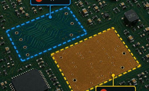
Concurrent power integrity analysis
The approach’s core concept involves designing the power distribution system (PDS) early to guarantee positive power integrity results from the beginning of the design process.
Other technology issues that reinforce the need to design, rather than simply create, include the need to provide charge over a wide frequency range, from low (e.g., system peripherals like disk drives) up to high frequencies moving into the GHz range. The ongoing lowering of supply voltages and noise margins of today’s ICs make the design of the PDS and definition of its target impedances a major design challenge.
Back when you as a designer only had to deal with a few voltages, extensive design work was usually not necessary to create a power distribution system. The overall board design process would start with the placement of ICs and the routing of regular traces, followed finally by a definition of the area allocated for the PDS. The final stage in this process was simply to connect all the ICs to the PDS.
But now, the increased complexity and density of boards means that this simple approach is just not as effective as it once was. The final stage is no longer just about connecting from A to B, because it is no longer physically possible.
With today’s complex boards the approach to incorporate different layers for different voltages has a knock-on negative impact on the cost of both design and manufacture. Alternatively, extra “fear capacitors” are often placed on a board in the final stages of design to achieve proper power integrity. Again, this increases cost in both additional components and manufacturing.
How to eliminate ‘fear capacitors’
The recommended option that eliminates the requirement of extra layers or “fear capacitors” involves designing the PDS first and then placing the other components around this – ensuring power integrity from stage one.
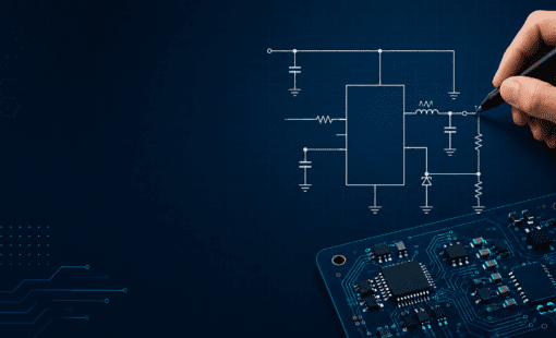
Concurrent power integrity analysis requires a fast analysis methodology, including what-if capabilities. Full-wave 3D solutions that can provide highly accurate results are unfortunately not applicable within the design process of most electronic systems where time-to-market and time-to-volume are key. A systematic approach that provides design arbitration to achieve a balance between conflicting constraints is essential. The concept is simple: Optimize the analysis time invested to achieve reliable decision making results.
In order to accomplish this, the EDA tools must manage the various design constraints with the ability to arbitrate between conflicting requirements.
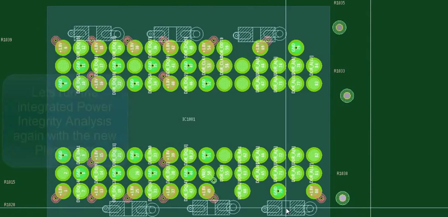
Car navigation system example
Consider a car navigation system that includes a very small board with a fixed form factor. The unit needs to fit into the radio slot in the car’s dashboard. Boards like these feature high-density IC technology such as uPGAs and CPUs, utilizing fast DDR2 memories and high-speed data links. The board also has to conform to a set power supply environment defined by the car manufacturer, and must comply to very strict automotive EMC limits. The challenge is then to fulfill all these demands to ensure power and signal integrity and guarantee EMC.
The PDS is designed at the beginning and all the components are then placed and routed using the initial PDS design.
Just as the quest for signal integrity in high-speed systems requires us to organize the topology of connections to achieve clean signals, the topology of power distribution systems must now be deliberately designed to prevent power integrity problems.
So you might be wondering what solution does this? And this is where I shamelessly plug our CR-5000 Lightning solution, specifically the Power Integrity & EMC Verification capabilities, that integrates analysis methodology into the layout phase of the design process and ensures a consistent set of design constraints.
Got a question on overcoming power integrity problems?
Feel free to get in touch with me or make a comment in the box below.

- Blog
- Blog
- Blog

- Blog
- Blog
- Blog
- Blog
- Blog
Related Products and Resources

- Products

- Products
Zuken’s engineering data management platform DS-CR has been created to support the specific demands of PCB design data management. It combines multi-site library, design data and configuration management into a unified engineering environment.

- Products
Building a competitive product today is much more difficult than a few years ago. Existing PCB-centric design processes are limited to a single PCB and do not provide the necessary tools for today’s competitive product development environment. PCB-centric design processes are falling behind.