
I Wish I Could Use PCB Design Software to Pack My Suitcase
Weren’t the summer holidays great?
Perhaps you had long warm days outside…time on your hands to spend with friends and family. Maybe even some rejuvenating sun, sea and sand.
But before all that there’s usually some hard work you need to put in before you get the relaxation payback. Planning, travel logistics and – unfortunately – packing.
With the event season now upon us, which started for me with PCB West, the travel ‘s about to begin again…
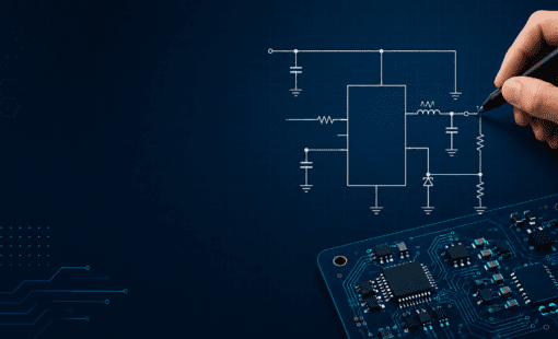
As we were preparing for PCB West, the idea of packing my suitcase connected with some of the cool new features in our product design software. Packing a suitcase isn’t that different than packing a product enclosure with electronics, battery, wires, connectors, etc. And one of our recent enhancements made packing the enclosure a lot easier. Designers can get a much more accurate product enclosure fit check earlier in the design process. The point is to avoid the heart-sinking (embarrassing and costly) moment that up to half of designers’ experience when they reach the prototype stage and realize something changed in the specification, and they now have a clearance problem in a hard-to-see corner of the enclosure.
The awkward shape problem
Thinking back to packing. I’d like you to cast your mind back to the last suitcase you packed. You probably have a default suitcase for your trip length. You laid out most of the things you wanted to take and tried to fit them in taking account of anything fragile, which maybe you wrapped in clothes. Then you grouped a few important items together in a bag like toiletries, glasses and medical kit. And you leave those shirts you’re hoping not to have to iron again until last – unless you’re a fan of the roll-it-all-up approach.
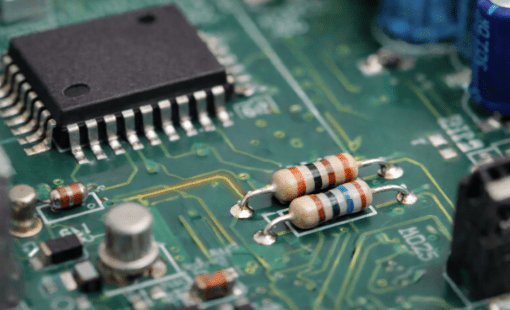
PCB layout designers have similar restrictions on where components can fit. They need to safeguard components with fragile connectors, for example, by avoiding touching the case or bending in areas with height restrictions, which could create a failure. They also don’t want to put sensitive components near heat sources.
There are always those component placements that have to take into account the shape of the enclosure – a bit like those annoying ingresses you get on the bottom of roller suitcases where the extending handles go. Then there’s PCB placement groups such as USB ports, which need to be easily accessible, and HDMI ports and power connectors, which generally go at the back of a product out of the way.
Accurate 3D vision
Of course when you’re packing your suitcase you have the benefit of a complete 3D view and you can see the exact size and shape of all the items. Closing the lid is not a problem.
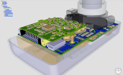
Which is a little like what you get with the latest update of CR-8000 Design Force. Instead of using stylized shapes defined by boundary boxes, CR-8000 Design Force now uses a true 3D component model with a precisely-matched 3D shape, making enclosure collision checks and 3D clearance checks much more accurate. And making fastening the enclosure lid straightforward.
If only I could use it to pack for Siemens Solid Edge University!
To find out more about getting clearance analysis to a true component shape, check out this movie:

-
Vice President of Marketing, Zuken USA, Inc.

- Blog
- Blog

- Blog
- Blog
Related Products and Resources
- Products

- Products

- Products
Zuken’s engineering data management platform DS-CR has been created to support the specific demands of PCB design data management. It combines multi-site library, design data and configuration management into a unified engineering environment.

- Products
Building a competitive product today is much more difficult than a few years ago. Existing PCB-centric design processes are limited to a single PCB and do not provide the necessary tools for today’s competitive product development environment. PCB-centric design processes are falling behind.