What You Really Need to Know When You’re Routing PCB Differential Pairs
You can tell when something isn’t as clear as it should be. The same questions come up time and again. You ask three experts and get three different answers. Routing a differential pair can be like that. Why? Because “it depends” – on exactly what signals those pairs are carrying and what kind of PCB you’re creating.
What can I tell you that’s useful? Well, I hope I can help to answer some of those repeat questions, so you can concentrate on the hard stuff.
Essential facts

Fan-out and end routing
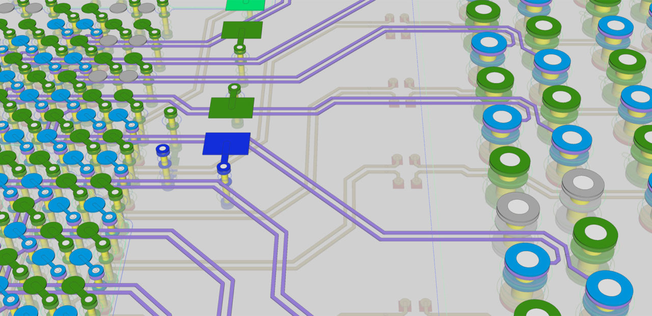
Let’s start at that differential driver on the left (![]() ). Imagine the TRUE (
). Imagine the TRUE ( ![]() ) and COMPLEMENT (
) and COMPLEMENT ( ![]() ) outputs are adjacent balls on a fine-pitch BGA, fanned-out to inner layers. Whatever else you do, keep the track lengths to fan-out vias equal, and then keep the lengths after those vias equal until you start the parallel track pattern. That parallel track pattern is the coupled section because there’s an electromagnetic coupling between the two sides.
) outputs are adjacent balls on a fine-pitch BGA, fanned-out to inner layers. Whatever else you do, keep the track lengths to fan-out vias equal, and then keep the lengths after those vias equal until you start the parallel track pattern. That parallel track pattern is the coupled section because there’s an electromagnetic coupling between the two sides.
Balance fan-out and end routing patterns separately at both ends. When you reach that receiver on the right, do the same as you did at the driver end. Don’t consider the lengths within the coupled section at all when doing this. Once TRUE and COMPLEMENT are coupled, the signals travel in a different way. I think of coupled sections as apples and fan-out and end routing as oranges – and you can’t add apples to oranges unless you want a fruit salad!
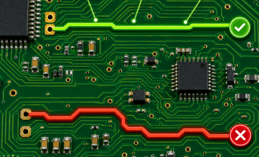
Corner angles and curves
If you only want good signal integrity, make no corner tighter than 135°. Many device application notes tell you the same. That angle works well for 45° routing. You’ll hear that curves give you better signal integrity, but for most PCB tracks – even for very fast signaling – that isn’t true. Get curves wrong and you’ll make it a whole lot worse – and what “wrong” means isn’t always obvious.
If you’re routing on a flex, you need curves, but that’s for mechanical reasons. You have to follow mechanical constraints, so the skill there is in making sure you don’t break signal integrity in the process.
Matching to other differential pairs
Add length in coupled sections only, and keep the pair coupled all the way because the differential impedance and delay-per-unit-length are different from the single-ended values – even within the same pair.
Matching between a differential pair and single-ended signals
In this case, you almost invariably need to add length to the pair, not the single-ended signal. As with matching between pairs, add length in coupled sections only. The application notes or standards docs will tell you how much.
Matching within a differential pair
Now you’ll remember that we matched the fan-out and end routing separately, so that’s not what I’m talking about here. This is about differences that arise within the coupled routing sections. This is sometimes called phase matching. The ideal is that TRUE and COMPLEMENT travel together in perfect complementary harmony, as shown on the left in the pictures below. There’s no such thing as perfection, so we get as close to it as we can. The faster your rising and falling edges get, the fussier phase matching requirements become. When slower edges get out of phase, the phase difference doesn’t affect the signal so much. You can see that in the pictures in the center and on the right. The phase difference matters most when TRUE or COMPLEMENT change state from low to high or high to low.

Differential impedance and delay-per-unit-length depend on phase matching. Without it, those numbers are different. To get good signal integrity, you need pretty good matching. You shouldn’t be breaking out from the coupled pattern, so the usual culprits where phase mismatches are concerned are corners. The outside track goes a bit further than the inside track.
The trap is to think you can just add the differences in length to the shorter sides, somewhere near the corners. Those are sometimes called phase bumps. There’s more to it than that, because the bump couples differently and the coupling round those corners gets quite fuzzy. You have to follow tight recommendations for exactly what those bumps should look like. If you don’t really need phase bumps, then my advice is not to add them.
The best place to start is to balance the number of 135° right and left turns and to try to minimize the number of turns. After that you can compensate for any remaining difference with a phase bump if you need to.
The real world
These PCI Express signals are making their way from a high-speed FPGA I/O bank to their connector. I guess you can see there’s a lot more to consider besides what I’ve mentioned, but I’d like to think this short blog post has helped answer a few of those golden-oldie differential-routing questions.


- Blog
- Blog
- Blog
- Blog