Exploring the Future of AI-Based PCB Design Solutions
Exploring the Future of Circuit Board Design. Can AI-based PCB Design Really Happen?
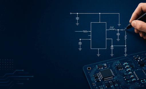
Printed Circuit Boards (PCBs) are the backbone of almost all modern electronics, from smartphones to sophisticated aerospace systems. Traditionally, PCB design–specifically, placing components and routing connections–has been a meticulous task requiring specialized knowledge and experience. With the advent of Artificial Intelligence (AI) and machine learning technologies, a question often arises: Can AI take over the complex task of placing and routing a PCB design?
This post will consider the current state of AI applications in PCB design, their advantages, limitations, and what the future might hold.
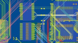
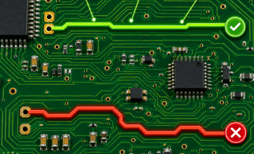
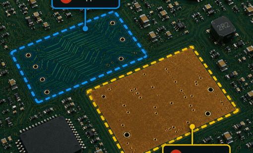
What is PCB Place and Route?
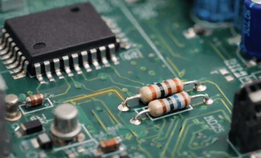
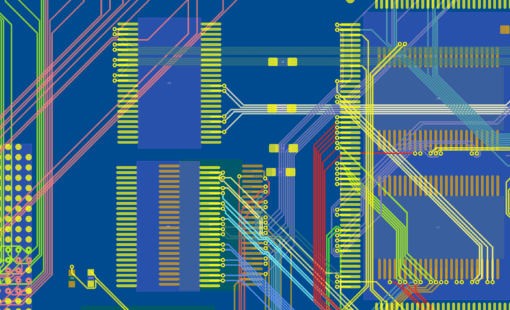
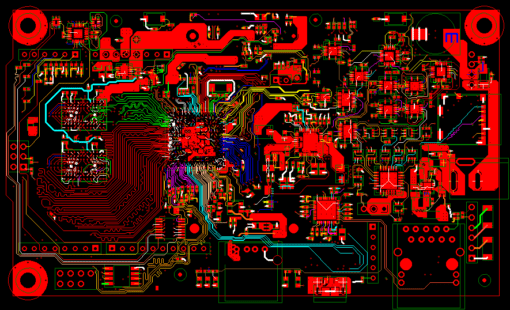
Before diving into the role of AI, let’s make sure we have a common understanding of place and route. Placing is the process of determining the optimal location for each component on a PCB layout. Routing involves drawing precise paths for electrical connections between these components while maintaining physical and electrical rules. Both processes are critical for ensuring a PCB is functional, efficient, and manufacturable. Errors in either process can lead to dysfunctional circuits, overheating, or higher production costs.
Why is AI Playing a Role in PCB Layout?
Typically, you will find specialists working on complex PCB designs. These specialists place and route PCBs as a profession. They have years of experience in developing best practices, making each new project as good or better than the last. Unfortunately, this generation of specialists is retiring–with no plans to replace them.
The current generation of engineers has their hands full, keeping up to date with the fast-moving technology trends. Designing a complex product involves multi-discipline expertise, and the art of PCB place and route is not a high priority for a number of reasons. For one, the task of placing and routing a PCB is a small part of the overall product development process. The expectation and hope are the PCB tool should be able to place and route the entire PCB with little human intervention. AI-based PCB design is the answer.
AI-based PCB Design: The Current State
Several companies and researchers are exploring the application of AI in automating the design and optimization of PCBs. The primary approaches under consideration include:
- Genetic Algorithms: These are inspired by the natural selection process and are used to evolve better solutions over successive iterations.
- Machine Learning Models: Trained on existing high-quality PCB designs, these models attempt to generalize the principles behind good design practices.
- Optimization Algorithm: Often coupled with AI, these algorithms focus on specific tasks like space utilization, power efficiency, or signal integrity.
The Future of AI-based PCB Design
The role of AI in PCB design is an evolving landscape filled with exciting possibilities and challenges. Although we’re not at a point where AI can completely replace human expertise, it has proven to be a valuable tool for augmenting our capabilities. As algorithms improve and our understanding of both AI and PCB design deepens, the collaboration between man and machine will only get more sophisticated, leading to quicker, more efficient, and perhaps even more creative solutions in PCB design.
So, can AI take the wheel in placing and routing PCBs? Maybe not entirely, but it can certainly share the driving.
Plans for an AI-based PCB Design Solution
Is Zuken working on a solution? Yes! Zuken is actively developing an AI-based place and route solution for the CR-8000 platform. Unlike other companies, Zuken has a long history of innovation with decades of experience developing and delivering advanced PCB design and layout solutions. AI makes perfect sense as the next step for Zuken. Machine learning is the basis for Zuken’s groundbreaking solution. With extensive experience and a vast library of design examples, this approach will deliver a robust solution applicable to a broad user base.
But many companies may prefer to learn from their own designs rather than from Zuken’s. This request makes perfect sense to us. In response, Zuken is taking a unique three-stage approach to AI-based design.
Key Advantages of Zuken’s Three-Stage AI Approach:
- Learning sources transfer best practices to new projects
- Enhanced collaboration between AI insights and human expertise
- Accelerated design iterations and reduced time-to-market
- Continuous self-improvement and evolution of AI capabilities
- Seamless integration into Zuken’s advanced CR-8000 platform
Into the Future of PCB Design
The evolving landscape of AI-based PCB design offers exciting possibilities and challenges. While AI will never replace human expertise entirely, it is proving to be a valuable augmentation tool. As algorithms and our understanding of AI and PCB design deepen, collaboration between humans and machines will become more sophisticated, leading to more efficient and innovative PCB design solutions.
Zuken is excited to announce the recent release of AI Place and Route for CR-8000. The innovative 3-stage approach is used into the future of PCB design. Learn more by reading our Press Release.

-
Vice President of Marketing, Zuken USA, Inc.

- Blog
- Blog
- Blog
- Blog
Related Products and Resources
- Press Release

- Products
- Products

- Products
Building a competitive product today is much more difficult than a few years ago. Existing PCB-centric design processes are limited to a single PCB and do not provide the necessary tools for today’s competitive product development environment. PCB-centric design processes are falling behind.