
Design Discipline Convergence Continues with the CR-8000 2017 Release
If you haven’t noticed, the electronic design process is evolving with the rise of Model-Based Systems Engineering (MBSE) and the demands of the Internet of Things (IoT). The standard 2D single board PCB design process can’t keep up with the demands of system-level design required by today’s more complex products. At the detailed design phase, we are seeing design discipline convergence where the boards and the enclosure are viewed as a single system. At the product level design phase, we are seeing the insertion of an MBSE and architecture design phase. The basic detailed design to manufacturing process isn’t cutting it. So while detailed design is converging, the design process is expanding.
Supporting system-level design abstraction
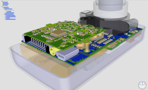
The standard 2D single board PCB design process is being replaced by a 3D multi-board design process; a multi-board product can be designed as a single system. At the same time, the MCAD design process is converging with the new PCB design process. This short video of Zuken’s CR-8000 PCB design platform demonstrates that convergence and it is worth a quick look. If you are still using a 2D design flow, this is essentially the next generation PCB design platform. The term “platform” seems much more appropriate than “tool” when we consider this is moving towards system-level design rather than simply one PCB at a time. The video nicely illustrates that at the detailed design phase, the design disciplines are converging and the design silos are being removed.
Earlier I mentioned the design process expansion with MBSE and architecture design. More on the MBSE design process expansion in a later post. For now, let’s look at the architecture design phase. You may not be aware, but the CR-8000 platform contains a hardware architecture design solution that fits nicely between MBSE and detailed design. The architecture design platform, System Planner, provides all the elements to design a multi-board system with consideration for mechanical fit, cost, weight and much more. This is another example of the design discipline convergence that was discussed above regarding detailed design. The architecture design phase supports a system-level design abstraction, as does the 3D multi-board detailed design process described above. Given this system-level approach, the architecture and detailed design tools can share data – major productivity benefit.
Connecting electrical and electronic design domains
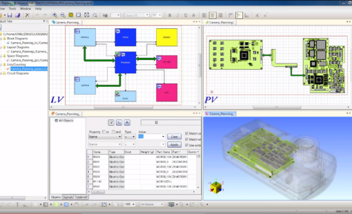
Now to the 2017 release of CR-8000 and more design discipline convergence. CR-8000’s hardware architecture design solution was originally built as a multi-discipline architecture design tool for electronic design (i.e., PCB-based systems). Now with the release of 2017, that bridge between electrical and electronic design has been built. Boards can now be connected by wire harnesses, (see figure 1) opening the door for more complex system-level design.

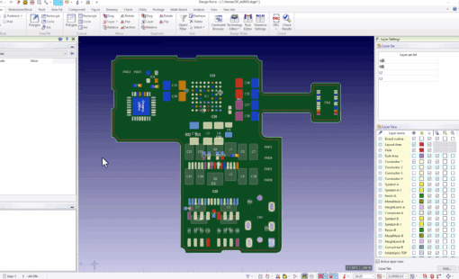
Figure 1: System Planner
Figure 1 illustrates how PCBs can be connected with a flex board or a wire harness. At the system architecture level, CR-8000 can now span electrical and electronic design domains. As products become more complex, we are going to see an increasing need for architecture design tools. The risk of entering detailed design without a sound and verified architecture is too high.
Now the really cool part…after you have optimized your PCB and wire harness architecture, your results move effortlessly into the detailed design tools. One of the biggest obstacles to the adoption of architecture design tools was the need to re-enter the design data into the detailed design tools. That obstacle has been removed. The wire harness design moves into the E3.series product for detailed design, while the PCBs move into CR-8000 Design Force for detailed design.
Gone are the days of working in silos
In conclusion, the growing need for a system-level design abstraction is driving the design discipline convergence. The cross-discipline dependencies are too significant to address with traditional silo-based methodologies. So the adoption of the next generation design process is being driven by the demand for a system-level design abstraction.

-
Vice President of Marketing, Zuken USA, Inc.

- Blog

- Blog
- Blog
- Blog
Related Products and Resources
- Products
Design Force offers an intuitive, integrated environment for designing single and multi-die packages for wire-bond, flip-chip, and high density advanced packaging. Designers can start designs with early prototype input of chip and package data from the library, reuse data from IC layout tools, and take advantage of parametric wizards to streamline the creation of the system

- Products
Zuken’s engineering data management platform DS-CR has been created to support the specific demands of PCB design data management. It combines multi-site library, design data and configuration management into a unified engineering environment.
- Products
Design Force combines traditional 2D design with native 3D design and the latest human interface techniques, accelerated graphics and almost instantaneous rendering and refreshing. It is the fastest, most effective PCB design solution available today. Design Force enables design teams to layout their designs in the context of a complete system or product.
- Products
System Planner provides a system-level design environment for the architectural planning and optimization of electronic systems and products. It enables engineers to optimize partitioning and performance of multi-board systems and maximize design reuse, while eliminating the need to re-enter up-front planning data into the design tools during detailed design.