
Routing JTAG: Ensuring a Successful Layout of Our Favorite Debug Interface
JTAG is one of those words that transitioned from a noun to a verb over time. I think we’ve all experienced the occasion when something isn’t working quite right and someone chimes in with, “well, you should JTAG that.” (In case you’re wondering, it is called an anthimeria when a noun is used as a verb, like googling.) Such is the power of JTAG that it made the transition from a capability to an action. Unless you’re working on a tried and true mature and robust design, you probably have JTAG on your board somewhere. While not a high-speed or particularly complex interface, laying out and routing JTAG is not without its nuance. We’ll look at some of that in this post so that you, too, can JTAG successfully.
Some JTAG Background
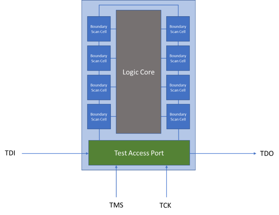
Microprocessors use sequential logic, which effectively means that between stages of combinational logic, there are flip-flops that hold the state of the previous step—the output clocks over to the next stage. One of the benefits is that with a little bit of additional hardware, you can introduce any arbitrary data you want into those flip-flops and get the processor into whatever state you want. Doing so is called boundary scan, and the Joint Test Action Group (JTAG) developed the IEEE 1149.1 standard for executing boundary scan.
Very simply, JTAG boundary scan acts like a big barrel shift register pushing data through at a known rate. That makes for a straightforward interface with only four pins: Test Mode Select (TMS), Test Clock (TCK), Test Data In (TDI), and Test Data Out (TDO). There is also an optional Test Reset (TRST). ARM offers a boundary scan capability using only two wires, but it still works similarly to JTAG.
JTAG Connection Topology
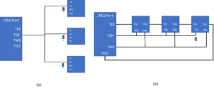
If you have multiple JTAG-able devices on a PCB, there are two ways to connect them. Firstly, thanks to the shift register nature of JTAG, you can daisy-chain them together where the TDO from one device connects to the TDI of the following device down the chain. This is perhaps the most straight-forward method for routing JTAG with the fewest layout issues.
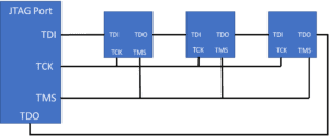
The second type of JTAG topology is what’s known as a star connection, where one JTAG connector is wired simultaneously to the JTAG ports of multiple devices. The daisy chain connection is the easiest one to implement, but it requires that all the devices in the chain have the same operating voltage. If there are devices with different voltages to debug using JTAG, it’s necessary to use the star connection with level shifters.
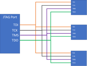
Devices have independent addresses, so only the target device will respond to JTAG commands, even in a star connection.
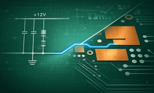
Considerations for Routing JTAG
JTAG isn’t a particularly high-speed interface, and if you’re debugging, you’re probably not too concerned with noise, but that doesn’t mean you can run wild routing JTAG; there are still some layout best practices to keep in mind.
- Crosstalk can be an issue between the control signals (TMS, TCK) and the data signals (TDI, TDO).
- It’s generally good practice to separate TMS and TCK by a ground plane.
- Route TDI and TDO predominantly on one of the exterior layers. One benefit to this is easy access as part of the test infrastructure.
Have you ever tried having a layout conversation with a transmission line person without uttering the word “stub”? Well, routing JTAG is no different. The JTAG clock signal benefits from having an impedance matching RC circuit. Placing that RC circuit incorrectly creates unnecessarily long stubs that could impact how the JTAG system operates. Ideally, you’d want to place the RC match at the furthest point of the daisy chain. In the case of a star connection, you can place terminations at the end of each clock signal location.
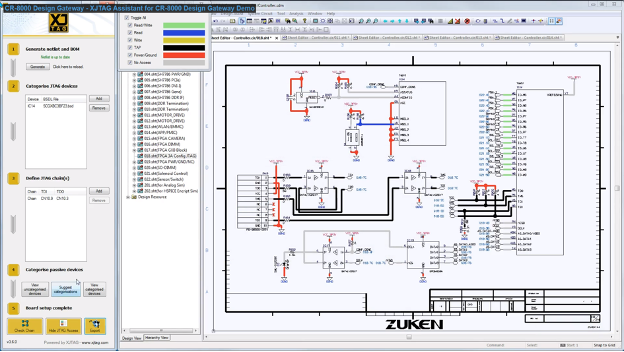
Making JTAG Easier with CR-8000 and XJTAG
As you can see, JTAG is a compelling debug interface that comes with caveats and considerations. The addition and cooperation of multiple “smart” devices that often have processor cores is the primary driver determining the complexity of today’s devices. Each of those can be elements with firmware and the typical bugs that come with software. The JTAG Boundary Scan interface is an excellent way to view the inner workings of those devices. XJTAG is a utility that runs from within the CR-8000 EDA tool suite. It automates checking the JTAG rules enabling successful implementation of design for test (DFT). In addition, XJTAG also facilitates the use of the debug interface without having to debug the debug interface. Click here to download XJTAG to your CR-8000 installation today and have peace of mind in your debugging.
- Blog
- Blog
- Blog
- Blog
Related Products & Resources

- Press Release
- Blog
- Products
- Products
Building a competitive product today is much more difficult than a few years ago. Existing PCB-centric design processes are limited to a single PCB and do not provide the necessary tools for today’s competitive product development environment. PCB-centric design processes are falling behind.