
PCB Stack-up Design Rules
Guest Contributor: Amit Bahl, CRO Sierra Circuits
Multilayer PCBs are part of modern electronics, which is advancing into miniaturization with complex and high-speed functionalities. Circuit boards are stacked with prepregs, copper foil, and core producing a sequential layer arrangement known as stack-up. A well-designed stack-up eliminates multiple issues like EMI, EMC, crosstalk, and impedance mismatching. Here, we will discuss the important PCB stack-up design rules for building an optimal build-up.
A brief overview of stack-up
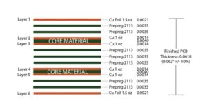
A stack-up represents the structure of a multilayer PCB in a sequential manner. It delivers crucial data, including material thickness and copper weights required for circuit board fabrication. It also shows the details of trace widths for different controlled impedance traces like 50 ohms, 100 ohms differential, etc. An example of a six-layer stack-up is below.
PCB stack-up design rules
The design or arrangement of a stack-up influences board fabrication and assembly. Fabrication requires determining the number of layers, their layout or build-up, and material type. These options establish a balance between thicknesses constraints, material parameters, including coefficient of thermal expansion, dielectric constant, electrical strength, signal type isolation, and drilling choices.
It is crucial to choose the right via routing option and understand how it impacts the stack-up. Let us now see the factors that affect the design of the stack-up.
The number of signal layers
The number of signal layers present in the design influence board build-up. These layers vary depending on the intended application of the circuit board. For example, high-speed signal or high-power applications may require more layers than low-speed signal applications.
Low-pitch and high-pin count complex devices, such as BGAs, typically require more signal layers. Signal integrity requirements like extremely low crosstalk may also result in an increased number of signal layers.
In the case of mixed-signal type, a separation between analog and digital signals is required, which leads to the increased count of signal layers.
A signal and power layer estimation tool will help gauge the number of signals required for the design.
The number of power and ground layers
The use of ground and power planes enables designers to assign signal layers solely for signal routing. These planes also decrease the DC resistance in power and ground rails, thereby assuring low DC voltage drop at the devices.
The ground layer is the plane of copper (copper pour) in the board that links to the ground connection of the power supply. A power layer is a flat plane of copper attached to the power supply rail.
The planes also provide high-frequency and time-varying signal return paths. Additionally, they assist in reducing noise and signal crosstalk, leading to improved signal integrity. Power planes also enhance the capacitive decoupling ability of the circuits. They also minimize EM radiation and improve EMC performance.
Trace width and spacing
The most challenging part of the layout is routing BGA packages. PCB designers should determine the signal count to be routed between vias in the breakout area. It will decide the minimum trace width and spacing to use. It is important to have a minimum line width to check any negative impacts on signal quality.
Controlled impedance traces
A circuit board trace and its corresponding planes form the characteristic impedance of a transmission line is known as a controlled impedance trace. A uniform controlled impedance is vital for achieving good signal integrity.
When the reference plane is not present on the next layer, there is a risk that another copper feature on the next layer will become the reference. Keeping a uniform etch across the length of the line, including the width and trapezoidal effect, is necessary from a manufacturing standpoint. That is the reason why etching tolerances and uniformity are vital.
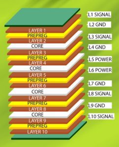
Sequential layer arrangement
Sequential layer arrangement is one of the critical elements of the stack-up design. One of the key factors to be considered before routing is the arrangement of high-speed signal layers according to the thickness of microstrips. The placement of signal layers near the ground/power plane will lead to tight coupling.
For precise layer arrangement:
- Maintain a minimum distance between power and ground planes.
- Avoid placing two signal layers adjacent to each other.
- Build a symmetric stack-up of the top and bottom layers inward.
- Use microstrips over dielectric material with a minimum dielectric thickness (approximately 3 mils) for high-speed routing.
Limiting the lamination step count in sequential lamination is crucial since it becomes expensive and time-consuming.
Determining layer material types
The thickness of each signal layer is a critical element for a build-up. Determine the thickness simultaneously while specifying the thickness of the prepreg and core. For different circuit board materials, there are standard thicknesses and other characteristics. It’s necessary to consider mechanical, thermal, and electrical properties while choosing materials. Typically, 0.5-ounce copper is used for signals, 1-ounce copper is utilized and for power planes. For high-current applications, 2 ounces of copper is used.
Sequence of stack-up
The recommended sequence is signal, ground/power, signal, ground/power, and so on. The best practice is to route the high-speed signals between two ground planes in the inner layers and on the ground references in the outer layers.
Determining vias
Determining the vias involves placing vias, the type of vias to be implemented, and copper weights. This step should be done with the contract manufacturer to make error-free stack-ups.
Some designs may require blind and buried vias. The size of the vias will depend on the thickness of the dielectric and the sequential lamination of the board.
Loss tangent and dielectric constant of the PCB material
Loss tangent (tan D) is a property of a dielectric material that characterizes the signal loss throughout the material. Whenever possible, choose materials with a lower loss tangent if you need to deal with long lengths and high speeds. Loss tangent affects trace loss significantly at high frequencies.
Sequential lamination
The sequential lamination process consists of sequentially building up a circuit board by adding layers of dielectric material and copper. Each layer is built upon subcomposites (subparts), which are structures composed of alternating copper and dielectric layers enclosed by a top and bottom copper layer. During lamination, a dielectric layer is sandwiched between a copper layer and laminated sub-composites.
Typically, sequential lamination comprises a core lamination and laminations built on top of this core consisting of alternate dielectric and copper foil.
Best practices for sequential lamination include:
- Select high Tg materials
- Minimize copper weights
- Place thin resin layers next to copper layers
Stack-up recommendations
Here are a few tips to produce an efficient stack-up design:
- In sequential lamination, every layer requires extra processing time. Thus, the number of sequential laminations increases cost and delivery time. Therefore, it is best to limit the number of sequential layers to three or fewer.
- Stacked vias should be filled after each sequential layer. This increases manufacturing process stages and span. Hence, use staggered vias if there is a scope to avoid stacked vias.
- It is crucial to know between which layers the mechanical buried vias are to be implemented and the requirement of staggered and buried vias.
- Sequential lamination may not be suitable for all materials. Manufacturers need to verify the suitability of their materials for sequential lamination.
By following the above suggestions, you can design a technically sound build-up. It will also ensure good manufacturability of your PCB stack-up. You can try out Sierra Circuits’ Stackup Designer to design that perfect stack-up.
Sierra Circuits’ Stackup Designer

This Stackup Designer provides a list of cost-effective and desired layer stacks for your board design. These build-ups offer improved signal integrity by reducing electromagnetic emissions and crosstalk. An impedance calculator is integrated within this tool which you can use to compute the necessary impedance, trace width, and spacing values for any signal layer.
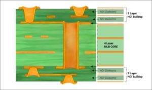
Below is an example of HDI stack-up generated using the Stackup Designer.
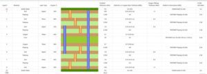
Main features of this Stackup Designer tool:
- Consists of a stack-up library which includes single and sequential lamination build-ups
- Linked to 2D field solver-based impedance calculator, which allows you to design controlled impedance boards
- Includes a wide range of material databases (Very low to high speed)
- Provides the cost index and technology levels (level 1/2/3). This gives you an idea of cost and technology level comparisons amongst the recommended stack-ups.
Conclusion
The optimal arrangement of board layers is one of the primary prerequisites for designing a reliable circuit board. If you’re working on a high-speed application, the placement of the ground planes is crucial to ensure signal integrity. Therefore, the goal is to optimize your build-up based on design aspects such as signal type, via structures, controlled impedance, and chosen dielectric material. You can learn more about these things in Sierra Circuits’ High-Speed Design Guide.
Guest Contributor: Amit Bahl, CRO at Sierra Circuits
Amit Bahl has been in the PCB industry for 25 years. Now Chief Revenue Officer at Sierra Circuits, his passion is to empower tech companies to achieve their visions and change our world. Rockets going into space, self-driving cars taking up the streets, cancer-fighting medical devices, protecting the country, he and his team help the best prototypes come to life.

- Blog

- Blog

- Blog

- Blog
Related Products and Resources
- Blog
- Blog
- Blog
- Blog