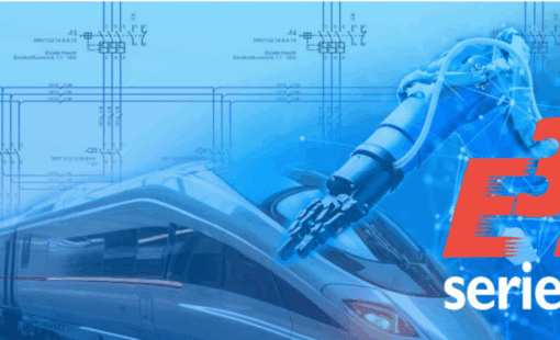
Engineering the Future: Zuken’s Role in Panel-Level Packaging Innovation
Why Panel-Level Packaging Is the Next Frontier
From smartphones to servers, modern devices demand ever-faster communication and smaller footprints. That puts pressure on every layer of semiconductor packaging, and Panel-level Packaging is emerging as a critical focus area. The interposers that connect chiplets are now at the center of this transformation.
Zuken has joined JOINT3, a pioneering consortium led by Resonac Corporation, to advance Panel-level Packaging through organic interposer development. This cross-industry collaboration is set to transform how advanced semiconductor packages are designed, manufactured, and verified.
What Is JOINT3?
JOINT3 (Jisso Open Innovation Network of Tops) is a cooperative R&D framework bringing together 27 global leaders in materials, equipment, and EDA tools. It serves as both a proving ground and a co-creation platform for innovations in semiconductor backend packaging.
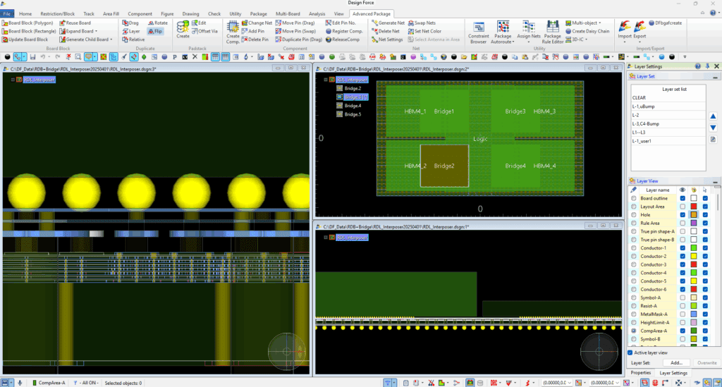
The initiative uses a prototype line for 515 x 510 mm panel-level organic interposers, offering a scalable alternative to conventional wafer-based approaches. This format promises better yield, lower cost, and higher performance.
Zuken’s Contribution: Turning Design Challenges Into EDA Solutions
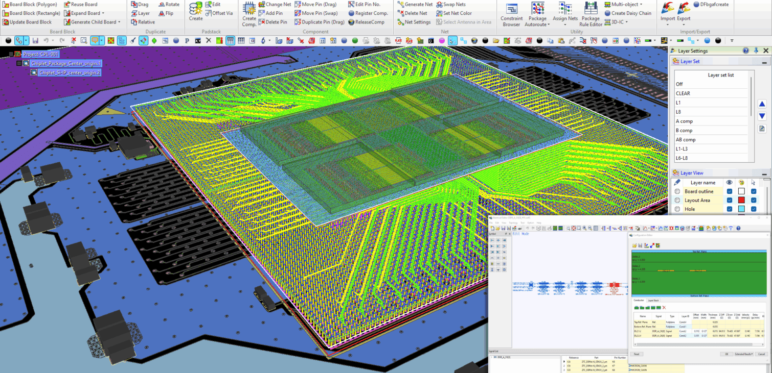
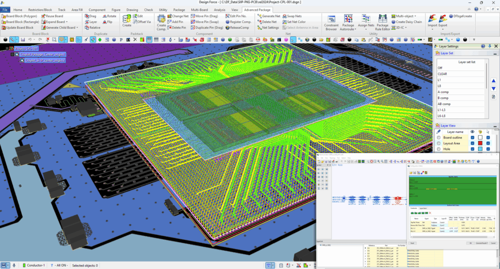
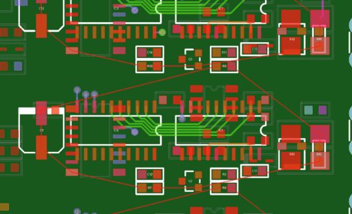
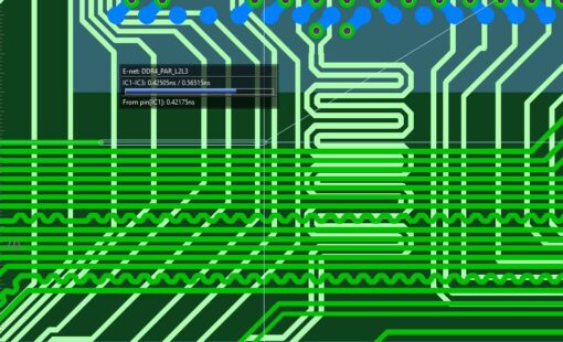
Zuken plays a pivotal role in JOINT3 by contributing advanced EDA tool development, design process validation, and multi-domain integration using our CR-8000 Design Force platform.
We’re not just observing, we’re building and validating real tools that help engineers solve real-world design problems.
Here’s how Zuken adds value to Panel-level Packaging innovation:
- Automating layout optimization for manufacturability in large panel formats
- Integrating electrical, thermal, and mechanical simulations into early design stages
- Supporting advanced architectures like Chip-on-Wafer-on-Substrate (CoWoS), 2.5D, and 3DIC
- Accelerating design validation with AI-assisted, simulation-driven workflows
- Enabling cross-domain collaboration between IC, package, and PCB teams
Why Panel-level Packaging Matters for the Future of Semiconductor Design
The shift to Panel-level Packaging with organic interposers isn’t just a technical upgrade. Instead, it represents a pivotal step that sets the stage for higher interconnect density, cost efficiency, and readiness for next-generation semiconductor designs. The benefits span multiple aspects of the design and verification process:
- Maximizing interconnect density with more cost-effective, and scalable organic interposers
- Lowering manufacturing costs through improved surface utilization compared to wafer-based packaging
- Extending scalability for high-volume production and long product lifecycles
- Enhancing reliability with better material and chemical property verification
- Maintaining system-level visibility to refine and verify interconnect paths
These advances bring exciting opportunities, but they also introduce fresh challenges from mechanical warping to signal integrity issues across larger substrates.

Design for Innovation: Zuken’s Vision
Zuken’s mission in JOINT3 is not just about keeping pace, it’s about leading with innovation. By embedding Panel-level Packaging support directly into CR-8000’s design and verification workflows, we help engineering teams:
- Collaborate across IC, package, and PCB domains
- Reduce costly rework through early-stage simulation
- Accelerate time-to-market through smart EDA automation
Final Thoughts: Toward the Next Semiconductor Era
JOINT3 is a rare example of deep, cross-industry collaboration, and Zuken is proud to be a contributor, not just a participant. Together, we’re helping define the workflows, tools, and standards that will shape the future of Panel-level Packaging and semiconductor innovation.
Learn More
Panel-level Packaging is redefining the future of semiconductor design. Zuken’s CR-8000 platform and our collaboration in JOINT3 are giving engineers the tools to innovate with confidence.

-
Manager of Engineering Operations, SOZO Center at Zuken USA Inc.

- Blog

- Blog

- Blog
- Blog
Related Products and Resources
- Blog
- Blog