
EMC for PCB Design: Anything but Black Magic
Electromagnetic compatibility (EMC) problems are often responsible for re-design cycles during the PCB design process. Due to ever shorter innovation cycles of electronic products like cell phones, or IoT applications such as fitness trackers or smartwatches, it is essential to avoid these time-consuming re-design cycles under all circumstances. In this post, I’ll walk you through the essentials of EMC for PCB Design. Once you understand the basics, you’ll see there’s nothing mystical about it.
EMC simply defined
EMC is the branch of electrical engineering and physics that deals with the unintentional generation, propagation, and reception of electromagnetic waves (in the E and H fields). These can all cause undesirable effects in electronic devices, including functional interferences, malfunctions, or even physical damage.
Generally speaking, there are two fundamental aspects to consider. First, the emission referring to the unwanted generation of electromagnetic energy and its transmission to the sinks, along with the necessary countermeasures to reduce such emission. And second, the respective susceptibility to interference relating to the operation of electrical/electronic equipment (or components) that become “victims” of unintended electromagnetic interference (EMI).
To simplify, EMC is the ability of electronic systems to function in a common electromagnetic environment without interfering with or being affected by other systems.
Know the potential EMI sources
On a PCB, there are various potential sources of interference that can cause a variety of possible effects:
- Signal and Power Integrity (conducted emission)
- Radiated emission
- Immunity to radiated and conducted emissions
- Electrostatic Discharge (ESD)
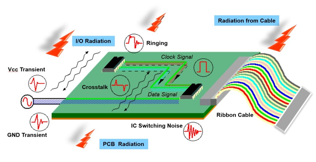
Often unnoticed by PCB designers, the ribbon cable on a PCB connector, for example, physically forms the arm of a dipole and thus creates a parasitic antenna. In this case, current and voltage peaks occurring during the switching process of the active components in the power supply can lead to an excitation of this parasitic antenna. This activity can result in an increased radiation pattern.
In addition, the signal-shapes in digital signaling are, in theory, ideal rectangles. But in reality, they don’t exist in such a form. Instead, the signals are created by adding up various sine waves containing high-frequency content. These signals more or less distorted and disturbed while traveling from driver to receivers. The resulting voltage peaks of the reflections and crosstalk will also have a negative effect on the EMC behavior.
Integrating EMC-compliant design into product development
EMC-compliant design is crucial to the success of a product. Only by complying with the EMC regulations of the specific target market or application (for example, the medical or automotive industry) can products gain approval for customer deployment in the first place. However, problems often only arise during the prototype testing phase, often due to a lack of properly integrated EMC verification procedures in the design process.
There are several options for managing EMC in the design process and detecting problems at an earlier stage. The first step is the systematic definition and use of design constraint processes, especially for signal and power integrity issues.
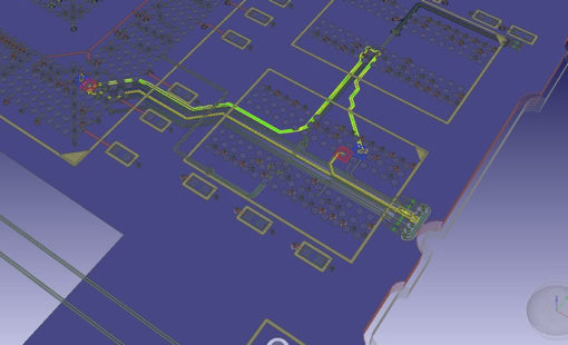
Introducing tool-supported EMC design reviews ensures adherence to the relevant EMC guidelines. CR-8000 Design Force includes EMC Design Rule Checks that enable selection or deselection of specific rules. These rules can also be prioritized on a per-user or per-design basis. The circuit designer can classify EMC-relevant signals for such checks early on during the schematic design process. The selected EMC rules suitable for an application are then applied during the PCB design phase.
The direct integration into the CAD process (2D and 3D) and the automatic generation of reports in the form of DRC checks–familiar to any PCB design engineer–simplify the workflow. These reports contain images, progress status, or approval information, and members of the development team can exchange them as Excel documents. This information is also stored in the design data for the joint work on EMC aspects in the design team.
The rules implemented in the EMC Adviser for Design Force contain recommendations for various design issues that enable non-experts to solve signal integrity, power integrity, and electromagnetic compatibility problems, thus developing an error-free, EMC-compliant layout. No additional software is necessary to validate the identified potential EMC issues.
EMC First Aid Kit for PCB Designers
For an EMC-compliant PCB design, it is essential to consider the following four areas:
-
Identify and evaluate parasitic antennas
It is essential to work out where parasitic antennas could form on the PCB. Parasitic antennas are developing electrical or magnetic monopole or dipole structures. -
Recognize and account for the current return paths
An electric current inevitably returns to its source. Therefore, visualizing the return paths and the return loops is critical. Depending on the application, the returning current runs along either the path with the lowest impedance or the path with the lowest resistance. In order to select a correct return path, do not wire lines across slots if possible, not even in differential pairs. -
Understanding various coupling effects
Coupling paths between the source and the sinks can occur depending on parasitic voltages, parasitic currents, or they may be IO-related. In many cases, their root causes are not immediately recognizable in the layout. -
Understanding resonances as potential antennas
Almost all electrical structures can become resonant. This includes single lines and differential signals, power supply structures, cables, packages, and even vias. Fortunately, it is easy to calculate the resonance frequency for many structures using this formula: fres=1/(2π√L∙C) However, knowledge of the values for the (parasitic) inductances (L) and capacitances (C) is not quite so easy to obtain and often requires complex analysis. Also, it is not possible to completely erase resonances. It is important to know and understand the effect and to avoid excitation where possible.
Conjuring the Magic
When it comes down to it, achieving EMC compliance in your PCB designs isn’t all that difficult. You have to first understand EMC and how and why it can affect your board designs. Then you need to know how to manage it. Using a tools like EMC Adviser and the CR-8000 PI/EMI tool speeds up the identification of EMC problems early in the design process eliminating costly re-design – and that’s where you’ll find the magic!

-
Product Manager/Senior Consultant

- Blog
- Blog

- Blog
- Blog
Related Products and Resources
- On-Demand Webinar
Electro-Magnetic Compatibility (EMC) is typically defined as the ability of a product to function in its environment without introducing electromagnetic disturbance.
- Products
Design Force combines traditional 2D design with native 3D design and the latest human interface techniques, accelerated graphics and almost instantaneous rendering and refreshing. It is the fastest, most effective PCB design solution available today. Design Force enables design teams to layout their designs in the context of a complete system or product.

- Blog