Are You Confident that Your PCB Subsystem Architecture Meets All the Requirements?
As products become more complicated, failure to meet the PCB subsystem architecture requirements can carry greater consequences than ever before. The subsystem architecture is the foundation of detailed design. Get it wrong, and the costs can be high. Architecture verification is a Digital Engineering design stage prior to detailed design. The product is decomposed into design tasks. Each task has a set of requirements that it must meet. The architecture verification stage is when the design team must determine that the PCB subsystem requirements are acceptable and manufacturable. This is no small task.
I chose to use the term “PCB Subsystem” versus “PCB design” because we can no longer design or verify a PCB in a vacuum. The PCB is part of a subsystem that includes the mechanical enclosure, interfaces to other subsystems, power, software, and sometimes chip/package/board co-design.
As products become more complex, new design methodologies (e.g., MBSE) decompose product requirements and assign them to architectural components of finer and finer granularity. A PCB subsystem or Electronic Control Unit (ECU) is one of those architectural components. Before starting detailed design, it is essential to ensure the PCB subsystem architecture is optimal and meets the requirements.
Start with the design envelope
The PCB and its associated parts must fulfill product requirements, including weight, cost, power, functionality, and performance. The systems engineering or architecture team essentially passes a “design envelope” to the detailed design team. The term design envelope is good because it infers design intent but not a specific implementation.
For instance, the design envelope provides a functional block diagram and requirements. The requirements would include the dimensions of the PCB subsystem or ECU. Let’s say we have a space allocation of 4”x4”x2”. Along with those dimensions are functional requirements. Functional requirements may include boot time, external communications, storage performance, sensor monitoring, etc. But the requirements don’t specify that implementation with one or two PCBs. That is a design decision driven by design exploration and requirements. But how do you figure out the optimal PCB count? It requires multi-domain considerations.
Time to make some decisions
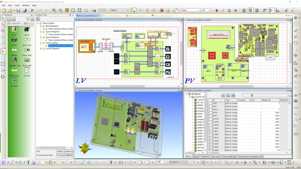
At this point, we are considering the design envelope and how to implement it. And as I said earlier, a wrong design decision at this stage can be costly. In many cases, you may receive a Visio architecture diagram and an Excel spreadsheet with requirements These tools are great for some tasks but not intended for systems design. Zuken’s design tool, System Planner, allows designers to quickly create and evaluate PCB subsystem architectures across domains. The proposed architecture is contained in four visionaries – logical, physical, space, and parameters. Designers can evaluate the architecture against requirements in each domain. For instance, the parametric visionary can create a composite BOM of the ECU or PCB subsystem to evaluate the cost.
Corporate library connection
A must for any PCB architecture verification tool is a connection to the corporate library. Without the components, 3D models, and functional blocks, doing the necessary analysis is impossible. System Planner allows you to quickly build a subsystem representation by using existing designs, approved components, and functional blocks without requiring all the details necessary to build it. Remember, this is not a detailed design. The gate to detailed design is to verify that the proposed PCB subsystem architecture fulfills the design envelope intent.
How many PCBs?
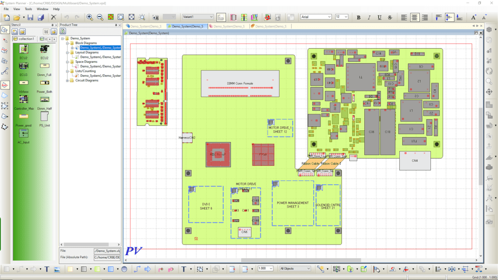
The PCB subsystem must deliver more and more functionality at a lower cost and with a shrinking footprint. System Planner allows you to consider a multiple PCB implementation by easily moving components from one PCB to the other and considering the ramifications (i.e., connectivity between boards and routability). It may be possible to reduce the original board count or size by logic consolidation, but there is a routability risk. Imagine meeting the requirements with one less board than expected–nice work. On the flip side, wouldn’t you want to identify an unroutable board now versus when you are in detailed design? System Planner can perform that analysis to help you make better design decisions.
Does it fit?
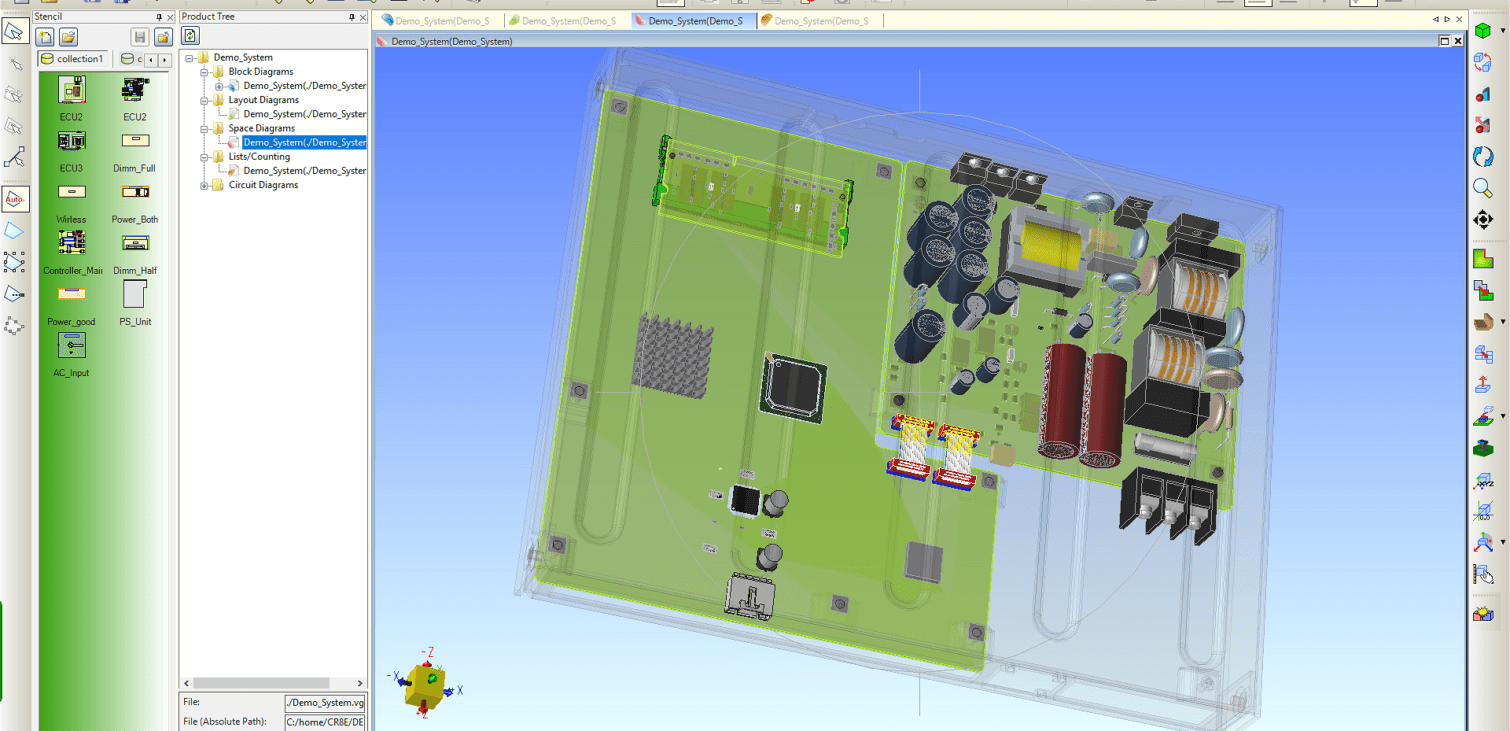
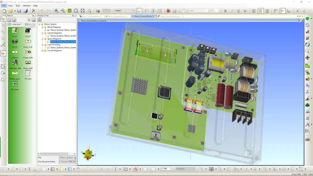
If I only had a nickel for every time I heard a story about the prototype boards not fitting into the mechanical enclosure! What a nightmare. System Planner allows you to import the enclosure directly from the MCAD tool, orient the board or boards, and perform clearance checks. Wouldn’t you like to know that the connectors line up with the enclosure openings and the boards meet clearance constraints? This is the digital twin at work!
How much does it cost and weigh?
We need to evaluate the entire PCB subsystem cost in the form of a composite BOM. System Planner rolls up the parts list, cost, power, and weight for the whole subsystem in a composite BOM. This BOM also includes the mechanical enclosure and board costs. And because System Planner is connected to the corporate library, if you are using any unapproved parts, they get red-flagged. The parametric analysis is another requirement verification tool to help you move to detailed design with confidence.
Off to detailed design
Now that we have verified the PCB subsystem architecture against the requirements and know it is realizable, it is time to move all this work to detailed design. This transition to detailed design is where many architecture tools hit the wall. Doing all this work knowing that you have to recreate the work in the detailed design tools is a show stopper.
However, with System Planner, it is literally a drag and drop action into Zuken’s 3D PCB design platform–CR-8000. CR-8000 is built for PCB subsystem or ECU design. It is native 3D and creates a digital twin of the ECU. Simply bring in the enclosure from your favorite MCAD tool (e.g., Creo, NX, SolidWorks, CATIA), orient multiple PCBs, and check clearances. Now you have a digital twin, all verifiable before moving to manufacturing.
Architecture verification is a necessary design stage
Product complexity and Digital Engineering are changing the way we design products. The document-centric approach is not meeting today’s needs. Design errors are becoming more common and have significant consequences. PCB subsystem architecture verification is just one example of how Digital Engineering can improve your design process by identifying design risk before detailed design. Look for more blog posts on the design stages and benefits of Digital Engineering.

-
Vice President of Marketing, Zuken USA, Inc.

- Blog

- Blog

- Blog
- Blog
Related Products and Resources
- Blog
- Blog
- Blog
- Blog