
8 Advanced PCB Design for Manufacturing Guidelines
Adhering to Design for Manufacturing (DFM) guidelines in circuit board design is crucial for efficiency and cost-effectiveness. Performing DFM checks prior to manufacturing can reduce the overall production cost by preventing costly errors early in the design phase. Moreover, it streamlines the production process by providing clear documentation, which minimizes manufacturing delays and the risk of needing to re-spin the board.
DFM ensures the efficient use of raw materials, leading to a more sustainable production approach. Finally, it facilitates scalability, making high-volume production more manageable through automated assembly and efficient soldering techniques, allowing for a smoother transition as demand increases. Involving your CM early in the design process improves communication and understanding across different manufacturing departments, leading to a more cohesive and successful project.
The team at Sierra Circuits shared their top 8 design for manufacturing guidelines to help you create a flawless PCB design.
1. Submit all the manufacturing files to your CM
The manufacturing data is checked to ensure it is within the manufacturer’s capabilities.
Make sure all these files are submitted to your CM:
| File name | What’s in it |
| Gerber/ODB++ file | Top and bottom overlays, solder mask, silkscreen, and drill drawing with hole diameter tolerances |
| Netlist | Name of the net, pin numbers, and reference designators |
| NC drill file | Drill sizes, hole types: PTH or NPTH, and tolerances |
| Component placement file | Information about the position and orientation of all SMDs |
| PDFs | Assembly notes, fab notes, stack-up, and impedance requirements |
| BOM | List of all the components to be assembled on the board |
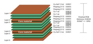
2. Ensure symmetry in your stack-up to avoid board warping
Consider these design guidelines when you’re building your stack-up:
- Verify if the selected materials meet the design requirements, considering Tg, dissipation factor Df, thermal conductivity (k), and mechanical strength.
- Ensure symmetry in your circuit board stack-up to prevent bow and twist.
- Avoid placing two adjacent signal layers to minimize EMI.
- Maintain a minimal spacing between power and ground layers to reduce impedance mismatching and minimize voltage drops.
- Choose foil construction for HDI boards. The foil layer provides a continuous ground plane, enhancing EMI shielding and heat dissipation. Additionally, foil construction simplifies trace routing and via placement, facilitating board miniaturization and increased component density.
- Accurate layer ordering and material thicknesses are essential for PCB functionality. Confirm that the layer stack-up aligns with the design intent and material thicknesses adhere to specified tolerances. This verification ensures efficient signal routing, impedance control, and thermal management.
3. Optimize the trace width and spacing as per the chosen copper weight
Opt for thicker conductor traces for higher current requirements
The trace width impacts the circuit board’s current-carrying capacity, controlled impedance, and signal integrity.
The minimum line widths for various copper weights are given in the table below:
| Start copper thickness | Minimum trace width in an outer layer (in mil) |
Minimum trace width in an inner layer (in mil) |
| 5 micron | 2 | 2 |
| 9 micron | 3 | 2.5 |
| ½ oz | 4 | 3 |
| 1 oz | 6 | 4 |
| 2 oz | 8 | 6 |
| 3 oz | 12 | 7 |
| 4 oz | 14 | 8 |
Manufacturers often choose the default trace width value, which may not be ideal for high-frequency and high-current applications. Therefore, depending on the specific application, the trace width is adjusted, thus impacting the conductor’s current-carrying capacity.

As per IPC-2221, the trace width for the specified current limit is calculated using the following formula:
I = (K) (𝝙T𝜷1) (A𝜷2)
Where,
I is the current in amp
𝝙T is the temperature change with respect to the ambient temperature in °C
A is the cross-sectional area in mil
K is the correction factor, which equals 0.024 in internal conductors and 0.048 in external conductors
𝛽1 and 𝛽2 are 0.44 and 0.75, respectively
The table below provides the maximum current-carrying capacity for 2 oz copper with a temperature rise of 10°C.
| Maximum current capacity (amp) | Minimum trace width for external layers (mil) | Minimum trace width for internal layers (mil) |
| 2 | 19.95 | 20.03 |
| 4 | 66.59 | 66.86 |
| 6 | 134.78 | 135.34 |
| 8 | 222.28 | 223.21 |
| 10 | 327.68 | 329.05 |
Maintain adequate spacing between conductors to prevent crosstalk
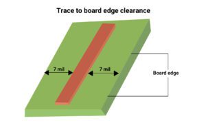
Inadequate trace-to-board edge spacing may expose the outer conductor to the external environment, making it vulnerable to corrosion. Furthermore, the trace is at risk of partial chipping during depanelization.
Always maintain at least 7 mil spacing between copper traces and board edges.
Maintaining a minimum distance between two conductors is essential to prevent crosstalk. Stick to optimum spacing between conductors based on the copper weight, as outlined in the table below.
| Start copper thickness | Minimum copper trace spacing on an outer layer (in mil) | Minimum copper trace spacing on an inner layer (in mil) |
| 5 micron | 3 | 2 |
| 9 micron | 3 | 2.5 |
| ½ oz | 4 | 2.25 |
| 1 oz | 6 | 4.25 |
| 2 oz | 8 | 6.25 |
| 3 oz | 12 | 8 |
| 4 oz | 14 | 10 |
4. Set the right aspect ratio and drill-to-copper clearance
The recommended aspect ratios for through holes and microvias are 10:1 and 0.75:1, respectively. Larger aspect ratios pose challenges in achieving proper copper plating within the vias, leading to increased manufacturing time and costs.
Therefore, higher reliability is associated with smaller aspect ratios. Always check the manufacturer’s capability before you finalize the aspect ratio.
The drill-to-copper clearance is the distance between the drilled hole edge and the nearest copper feature. This clearance is influenced by material resin content, weave structure, accurate positioning, and precision of the drill machine.

When determining drill-to-copper clearance, it is essential to consider the edge of the drilled hole. You can evaluate finished hole-to-copper clearance using the following equation:
Finished hole-to-copper clearance = drill-to-copper clearance + (plating thickness ✖ 2)
Recommended drill-to-copper clearance is 8 mil.
5. Ensure optimal annular ring to prevent tangency and breakout issues
Despite meticulously placing vias at the center of pads in design files, achieving the same precision in fabrication is often elusive.
Manufacturing complexities, such as off-center drilling during the lamination and incorrect hole registration, can lead to tangency and breakout.
Tangency: If there’s an insufficient annular ring, the drilled hole may nearly touch the pad’s boundaries, resulting in an annular ring width of zero. This tangency causes connection issues between the via and copper traces.
Breakout: An annular breakout occurs when the hole shifts over the copper pad during drilling, deviating the drill bit outside the pad. This breakout can cause connection problems between the via and the connecting layers and affect component placement and solderability.

To achieve optimal annular ring, always discuss with your CM before placing an order. Ensure the manufacturer can maintain the specified annular ring as indicated in the fab drawing. Copper pads must be present for plated drills on all copper layers.
As per IPC-6012, for class 2, a 90° drill breakout is allowed. On the other hand, the minimum internal and external annular ring cannot be less than 1 mil and 2 mil, respectively, for class 3 PCBs.
We recommend less than 2 mil annular ring for laser-drilled vias, while mechanically drilled vias need a minimum 3 mil annular ring.
6. Locate unconnected lines, undesired ground connections, and hairlines, if any
Verify if all interconnections are present in your PCB layout
One way to do this is to generate an IPC netlist from the schematic. This file will list all of the connections between the components on the board. You can then use this netlist to verify that all interconnections are present in the PCB layout.

If there are any missing interconnections, it results in open circuits.
Remove unintended ground connections
You should always eliminate unintended ground conductors and thin traces in copper-flooded areas. These traces can cause unintentional connections between components and can lead to circuit malfunctions.
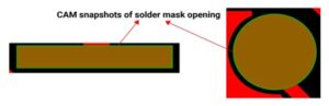
7. Ensure proper solder mask coverage to avoid solder bridges
Solder mask layers provide electrical isolation between components. Consider these design tips to avoid errors in solder mask:
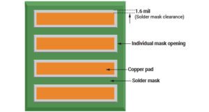
Incorporate sufficient mask clearance from the SMD pad
Solder mask clearance refers to the distance between the mask edge and the surface features on a circuit board. This clearance is crucial to prevent solder bridges. Solder bridges occur when molten solder flows between adjacent pads or traces, causing short circuits.
Conventionally, the recommended solder mask clearance around SMT pads is half of the conductor spacing width. This means that if the spacing between two pads is 2 mil, the clearance should be 1 mil.
However, PCB manufacturers often recommend a slightly larger clearance of 1.6 mil to provide a margin of safety.
Inspect for partially or entirely missing solder mask between pads
Thoroughly examine the PCB layout to identify instances where the solder mask is partially or entirely missing between pads. These gaps can lead to solder bridges, causing short circuits and circuit malfunctions. Ensure the solder mask covers all areas between pads, maintaining a consistent barrier.
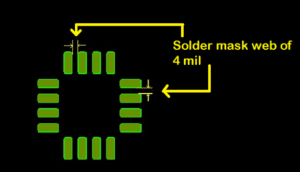
Maintain adequate solder mask web
The solder mask web should adhere to the specified minimum width. A minimum web width of 4 mil is recommended for green and red solder masks. For other colors, a minimum web width of 5 mil is advised. Maintaining the specified minimum web width ensures sufficient mechanical strength and prevents solder bridges.
Maintain more than 2 mil mask coverage
Implement solder mask coverage that exceeds 2 mil beyond the copper pads. This additional coverage provides a safety margin to accommodate manufacturing tolerances and misalignments.
Ensure adequate mask clearances in vias
Vias should have larger clearances in the solder mask than the hole diameter. Additionally, set solder mask openings in a 1:1 ratio with the copper pads. This prevents solder from bridging between the via and the adjacent copper traces.
Specify mask relief areas in your fab notes
Clearly specify the areas where the solder mask should be removed. These areas are typically found around heat sinks or components with tight pad spacing. Defining solder mask relief areas ensures the resist layer does not interfere with component placement and heat dissipation.
8. Make sure the silkscreen is legible
Silkscreen is a visual guide for component placement and identification. Adhere to these guidelines for legible silkscreen in your PCB:
Do not overlap reference designators
Reference designators should be carefully positioned beside the pad without overlapping. If not, it can hinder component identification.
Avoid silkscreen over vias and under components
Do not place silkscreen over through-hole vias. It can block access to solder points.
Similarly, do not place them under components since it can hide the necessary markings, making it difficult to solder.
Maintain accurate polarity markings
Verify polarity markings, which indicate the orientation of polarized components. Misaligned or unclear polarity markings can lead to component misplacement and potential circuit malfunctions.
Ensure optimal line width and text height
Silkscreen lines should have a minimum width of 4 mil to maintain visibility. Text height and length should be at least 25 mil to ensure legibility, especially for smaller components.

Choose a standard silkscreen color
Silkscreen is typically printed in white to maintain consistency and enhance readability. Using non-standard colors can make silkscreen markings less visible. Clearly specify the size of the company logos and dates in the fab notes.
You can run a check for all the above parameters using Sierra Circuits’ Better DFM Tool.
Validate your design with Sierra Circuits’ Better DFM tool
Sierra Circuits’ Better DFM tool checks for manufacturability of an electronic design. It simplifies the product design and enhances the functional performance of the circuit.
- Allows you to compare the IPC-356 netlist with the netlist file present in the Gerber.
- Provides advanced options for defining minimum annular ring and minimum drill-to-copper requirements.
- Offers automated solder mask and silkscreen optimizations to improve manufacturing efficiency. Solder mask optimization adjusts clearances to maintain required space, while silkscreen optimization ensures proper spacing from solder mask and pads.
- Accepts multiple drill files, and you can specify the plating type (plated or non-plated).
- Provides various reports, including DFM reports (for identified issues), netlist reports (for opens and shorts), and Gerber layers shown in PDF format.
- Integrated with Sierra Circuits’ PCB online service, enabling you to request an instant price quote.
Implementing design for manufacturing guidelines is a proactive approach that can lead to cost savings, time efficiency, improved quality, and a seamless PCB production process. It aligns design and manufacturing goals, resulting in a well-designed, practical, and economical product.

-
CRO at Sierra Circuits


- Blog

- Blog
- Blog

- Blog