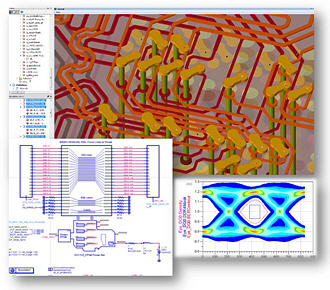
The ADS board link (ABL) enables a smooth transition from your Zuken flow to Keysight’s Pathwave ADS for simulation and analysis. Pathwave ADS is here to help you innovate game-changing technologies and to accelerate your workflow, whether it be for RF design or signal integrity/power integrity. ADS features such as SIPro are specifically designed for SI engineers to improve link performance in PCBs. With the net-driven interface, the designer can quickly select the nets they want to simulate together with the power and ground planes, including surface mount components. No time or effort is needed to manually edit connections prior to simulation. Easily incorporate the ABL link to streamline your post-layout analysis and to progress from layout to simulation results in less than 20 clicks.
SIPro utilizes a composite EM technology to deliver pure EM analysis with higher capacity than general-purpose EM solutions. SIPro captures all relevant EM effects such as:
Via-Via coupling
Via-Microstrip Transitions
Signal to Ground / Power Plane Coupling
Once the simulation is complete, the designer can quickly plot the following, enabling you to quickly assess whether the EM model is sufficiently characterized.
S-parameters (both single-ended and mixed mode)
TDR/TDT
Near end & Far end cross-talk
With a single click, automatic schematic generation back-annotates the EM model to an ADS schematic, making it ready to use in one easy flow, enabling a smooth and productive workflow.
PIPro Overview
Power integrity (PI) has become an ever-increasing challenge, driven by two main issues:
The need for higher device integration with lower IC supply voltages
Smaller PCB sizing leading to less space for wide power planes
Take your design into your own hands when it comes to power integrity analysis:
PIPro accounts for the real physical layout of the power delivery network (PDN), incorporating items such as plating thickness for vias. With a dedicated PI-DC simulator, you can get visual feedback in seconds on exactly what the voltage distribution looks like for the selected power and ground nets.
As power distribution networks (PDN) are forced into smaller spaces on the PCB, the power plane may not perform as originally designed due to the temperatures affecting the plane’s voltage drop. Solve this issue using the fully automated electro-thermal iterative simulation. Receive the most accurate representation of the DC IR drop by considering local resistivity changes due to heating, also giving you the ability to perform thermal floor planning.
ADS consider PI not only from a DC perspective but also from the perspective of switching frequencies and transient loads. With the need for flat impedance response, use the AC simulator to compute the PDN impedance versus frequency of the distributed layout with your decoupling capacitors in place. A flat impedance gives us the best opportunity to avoid a destructive voltage ripple in the PDN.
Completing the flow with the final system simulation
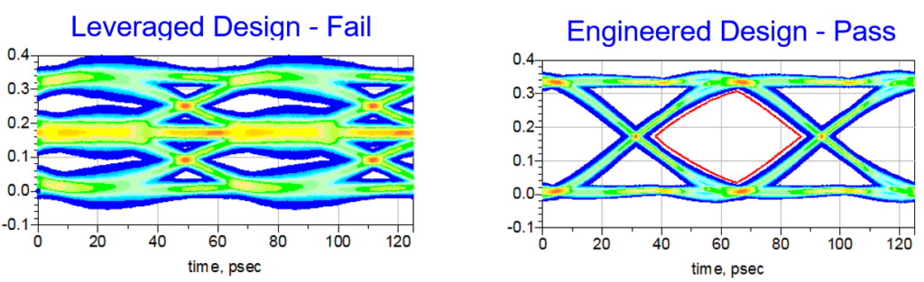
Use the automatic schematic generation that will back-annotate your EM model to an ADS schematic, making your design ready for use in transient and channel simulations, all in one easy flow. ADS’s channel simulation is here to address the generation of eye diagrams, bathtub plots, and eye contours measurement of margin-to-mask for extremely low bit-error-rates (BER), as demanded by high-speed link designs.
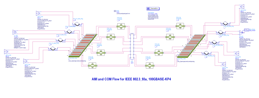
Simulate easily in early pre-layout phases with ADS’ generic receiver component, which can compute the optimum FFE and DFE for the receiver.
Mix and match different models from IBIS AMI and non-IBIS AMI, including SPICE. Rely on the industry’s leading channel simulation technology, enabling you to predict your margins with confidence.
Conclusion
With a fast and efficient transfer of layout artwork, component information and substrate stack up the ABL link enables you to access a powerful suite of simulation analysis tools in Pathwave ADS.