CR-8000 Design Force – Chip-Package-Co-Design
Chip-Package-Board Co-Design
Today’s advanced-node IC designs are challenging architects, designers and manufacturers to develop error-free and accurate data to produce right- thefirst-time market solutions. Lower budgets and price pressures are pushing formerly separate design silos into one of two design scenarios:
- Multiple re-spins with second and third turn optimization putting enormous cost and time-to-market pressure on design teams;
- Concurrent chip, package and board co-design with reliable, real-time shared design data continuously throughout the design and verification process;
Concurrent chip, package and board co-design provides lower package cost and reduces PCB cost through resultant layer reductions. Comprehensive system co-design recognizes the interaction between chip, package, and board data to reduce complexity, size and cost of the overall system. Zuken’s Design Force native 3D chip, package and board co-design enables optimization of the chip-package-board interface throughout the design flow to address these market advantages.
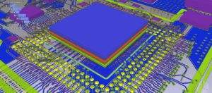
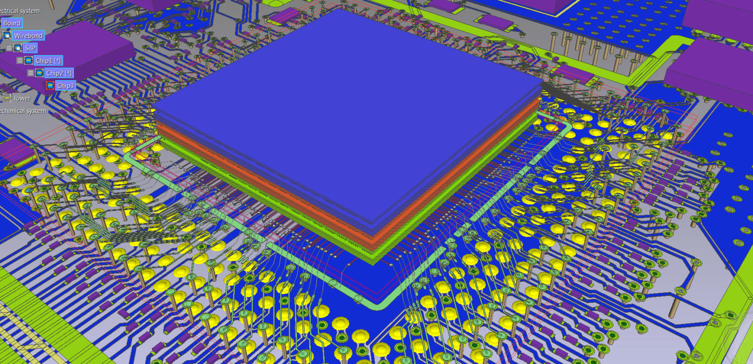
As the industry moves from coplanar designs to complex 3D stacked structures and embedded devices, the need exists for tools that can accurately render and provide meaningful visual and DRC feedback to enable, rapid right-the-first-time designs. Design Force’s inherent chip, package and board co-design capabilities enable realtime 3D hierarchical design, allowing design teams to concurrently create any combination of advanced stack dies, packages and PCBs.
In Design Force multiple co-design configurations for chip, package and board are supported such as SoC/package, package and PCB and SoC/System in Package (SiP)/PCB co-design. Design Force chip, package and board path finding solution uses industry standard OpenAccess die database to optimize system design. Users can also automate and configure rules-based perimeter I/O and area I/O planning and placement. The solution also provides bump planning/placement and a feature-rich die and interposer Redistribution Layer (RDL) and escape router.
Top features and benefits
- Multi-board constraint browser to view and analyze system level interconnects
- Automatic ball assignment with the ability to optimize complex routing solutions
- Interposers supported with throughsilicon-vias (TSV) and bidirectional support for exchanging System on Chip (SoC) information using industry standard formats
- 2.5/3D stacking structures handled in any configuration: stacked, adjacent, interposers, with wire bond and flip chip packages
- Rule driven I/O placement Redistribution Layer (RDL) router that supports 45 degree, multi-layer, and multi-region routing
- Rapid scriptable design and feasibility studies for die sizing; I/O placement (area and peripheral); bump planning, RDL placement, and escape routing
- Numerous routing engines enable rapid feasibility or detailed RDL and bump escape routing of signals and power and ground nets
Download Datasheet