CR-8000 Design Force – Advanced Packaging
Advanced Packaging – Design Force
Traditional two dimensional design tools often fall short when it comes to studying the structure and routability of the advanced packages required for today’s complex designs.
Virtual prototyping of the optimal floorplan is beneficial, along with the ability to access verification tools as early as possible in the process. Tools that support 3D system-level design, which also seamlessly connect with verification tools, can significantly improve the package design process.
A more intelligent approach to package design is one in which the chip, package and board can be designed simultaneously. Zuken’s Design Force native 3D chip, package and board co-design environment enables design and optimization of the interfaces between all three domains throughout the design flow.
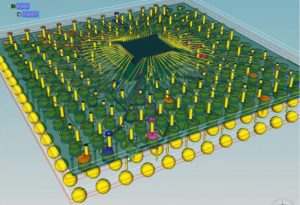
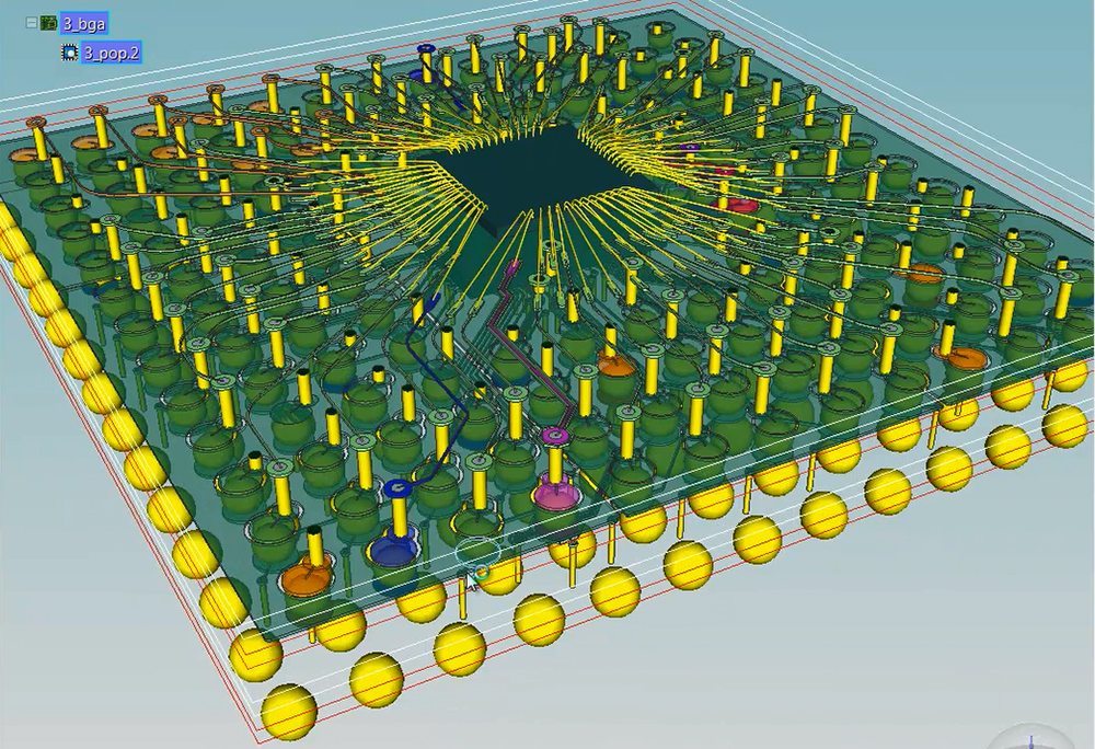
Design Force Advanced Packaging offers an intuitive, integrated environment for designing single and multi-die packages for wire-bond, flip-chip, and high density advanced packaging.
Designers can start designs with early prototype input of chip and package data from the library, reuse data from IC layout tools, and take advantage of parametric wizards to streamline the creation of the system. Design Force includes support of 2D- and 3D-based design and manufacturing rules to ensure the package is designed right-the-first-time.
With its native 3D platform, designers can easily implement and manage dense interconnects for wire bond or flip chip packages, and incorporate embedded component technology for advanced packaging and module design.
Top features and benefits
- Unified environment to handle packaging technologies, including chip scale packaging (CSP), multi-chip modules (MCMs), and system-in-package (SiP)
- Parametric wizards for chip and package structures reduce time and effort for implementing complex package designs
- Automatic ball assignment with the ability to optimize complex routing solutions
- Conduct feasibility studies and shorten design implementation with advanced fan-out/fan-in and autorouting features to optimize package layer count
- 2.5/3D stacking structures handled in any configuration: stacked, adjacent, interposers, with wire bond and flip chip packages
- Native 3D environment enables true rules-driven approach to ensure designs are implemented and verified accurately
- Hierarchical database allows users to conduct co-design with ICs and PCBs in one environment to realize the latest technologies, such as 2.5/3D IC design
Download Datasheet