Transitioning from Architecture Design to Detailed Design
On-demand webinar
This webinar is Part 3 of a 3 part series covering the systems engineering process of converting product or system requirements into a viable and robust hardware architecture and then moving that architecture directly into detailed design without any manual re-entry.
Architecture design is typically done with a variety of tools including Excel and Visio. Once an architecture is defined using these tools the architecture design must be realized in the detailed design process. That transition today is manual and error prone involving data re-entry.
This webinar demonstrates the seamless transition from architecture design and optimization to detailed design. After a short review of architecture optimization and validation, the design will be moved to detailed design. A functional block diagram becomes a detailed design schematic or schematics. 2D multi-board planning becomes a 2D/3D PCB design ready for detailed placement and routing. Data re-entry is not required.
What you’ll learn:
- How to easily transition from architecture design to detailed design without any data loss or re-entry
- Functional block transition to a traditional schematic or schematics
- 2D multi-board floor planning transitions to a multi-board system
Who should watch:
- Hardware engineers
- System architects
- Design engineers
- Electronic engineers
- Product managers
- Engineering managers
Related resources
- Press Release
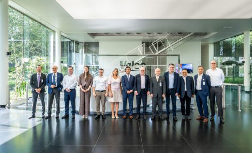
Valeo et Zuken collaborent à travers le Zuken Valeo InnoLab afin de créer une plateforme ouverte de conception électronique assistée par l’IA pour l’ingénierie automobile. Cette collaboration associe l’architecture IA de Zuken aux agents IA et à l’expertise industrielle de Valeo afin de réduire les délais de conception, renforcer la continuité numérique et soutenir une conception électronique robuste sur l’ensemble du processus de développement.
- Press Release
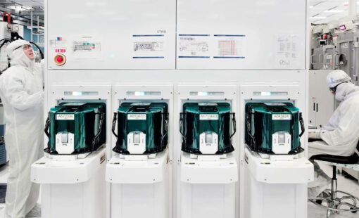
Zuken Inc. has joined the JOINT3 consortium—an industry co-creation platform led by Resonac to accelerate the development of next-generation semiconductor packaging materials, equipment, and design tools for panel-level organic interposers—where Zuken will contribute its CR-8000 Design Force expertise to help demonstrate, optimize, and evolve design and manufacturing processes that address the growing demand for 2.xD and 3D semiconductor packages in applications such as generative AI and autonomous driving.

- Press Release
Explore CR-8000 2025’s latest AI and simulation upgrades for faster, more reliable schematic and layout design—optimized for high-speed, high-density electronics.
- Press Release
Zuken a signé un accord de développement conjoint avec IBM pour innover dans l'intégration 3D des circuits, accélérer le hardware pour AI et optimiser les workflows EDA. Cette collaboration se concentre sur l'intégration hétérogène de puces, l'évaluation des accélérateurs d'apprentissage profond, let les tests de fiabilité. Ce partenariat souligne l'engagement de Zuken à stimuler l'innovation dans la conception de puces alimentées par l'IA et les solutions de packaging de semi-conducteurs de prochaine génération.