Participating in “JOINT3” Consortium to Develop Next-Generation Semiconductor Packaging
Zuken Inc. (President: Katsube Jinya, hereinafter “Zuken”) has joined “JOINT3” consortium to develop next-generation semiconductor packaging. JOINT3 is a co-creation evaluation framework established by Resonac Corporation (President and CEO: Hidehito Takahashi, hereinafter “Resonac”) with the aim of accelerating the development of materials, equipment, and design tools optimized for panel-level organic interposers through collaboration among material, equipment, and design companies. JOINT3 brings together global leaders in semiconductor supply chain. Using a prototype line for 515 x 510mm panel-level organic interposers, the consortium promotes the development of materials, equipment, and design tools optimized for panel-level organic interposers.
Based on Zuken’s track record and expertise as an EDA vendor supporting customers in advanced packaging design, we participate in the practical implementation of next-generation semiconductor packaging design, manufacturing, and verification with panel-level organic interposers in JOINT3. And Zuken contributes to the establishment of optimal design and manufacturing process by developing tools and features to solve issues that emerge in the process.
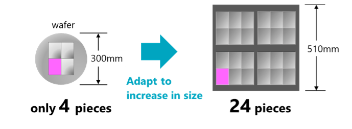
In recent years, packaging for back-end processes has emerged as a key technology in the field of next-generation semiconductors. This includes 2.xD packages, whereby multiple semiconductor chips are arranged in parallel and connected via interposers, demand for which is expected to grow in line with the need for increased data communication capacity and speed. As semiconductor performance improves, interposers are becoming larger, and there is a shift from silicon interposers to organic interposers made from organic materials.
Conventional manufacturing methods involve cutting rectangular pieces from circular wafers. However, as interposers increase in size, the number of them that can be obtained from a single wafer decreases, posing a significant challenge. To address this issue, a manufacturing process that transitions from circular wafer shapes to square panel shapes is gaining attention, as it allows for an increased number of interposers to be produced from a given area of wafer.
Zuken has participated in various 2.5D and 3D package design, manufacturing, and verification projects, in addition to providing customers with advanced package design environments. Throughout the course of these projects, we have a proven track record in supporting the design and tool development for various technologies such as Chip stacking, Organic Package stacking, and various interposers. These experiences and technologies are consolidated into the CR-8000 Design Force’s 2.5DIC/3DIC design and verification features, and the SoC/package/PCB collaboration design environment.
In JOINT3, Zuken engages in the practical implementation and validation of next-generation semiconductor packaging design and manufacturing using panel-level organic interposers. In addition to verifying the physical structure design and electronics design, Zuken is also planning to develop new functions such as preliminary verification in the design stage that takes into account the physical properties and chemical characteristics of various materials.
By collaboration and co-creation with other JOINT3 members, Zuken contributes to the evolution of design, manufacturing, and verification process for the next-generation semiconductor packaging with panel-level organic interposers. And Zuken aims to play a key role in the next-generation ecosystem and supply chain.
Overview of JOINT3
| Name | JOINT3 (JOINT:Jisso Open Innovation Network of Tops) |
| Objectives | Accelerate the development of materials, equipment, and design tools optimized for panel-level organic interposers through co-creation with participating companies. |
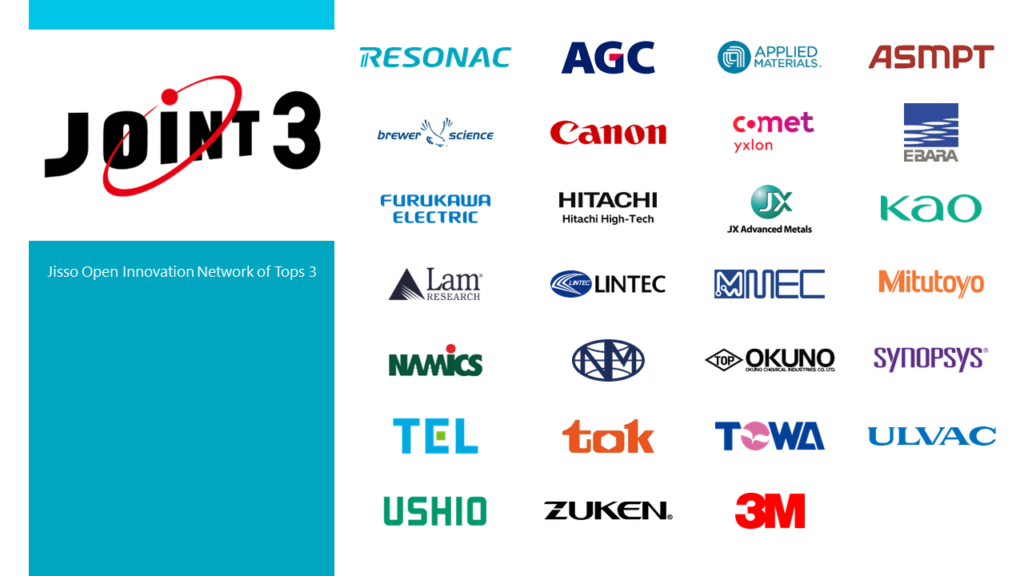
| Participating Companies (listed in alphabetical order) | 27 companies (as of September 3, 2025) |
| Resonac Corporation, AGC Inc., Applied Materials, Inc., ASMPT Singapore Pte. Ltd., Brewer Science, Inc., Canon Inc., Comet Yxlon GmbH, EBARA Corporation, Furukawa Electric Co., Ltd.,
Hitachi High-Tech Corporation, JX Advanced Metals Corporation, Kao Corporation, Lam Research Corporation, LINTEC Corporation, MEC COMPANY LTD., Mitutoyo Corporation, NAMICS Corporation, Nikko-Materials Co., Ltd., OKUNO CHEMICAL INDUSTRIES CO., LTD., Synopsys, Inc., Tokyo Electron Ltd., Tokyo Ohka Kogyo Co., Ltd., TOWA Corporation, ULVAC, Inc., Ushio Inc., ZUKEN Inc., 3M Company |
|
| Location | – Advanced Panel Level Interposer Center “APLIC” (Yuki City, Ibaraki Prefecture, Japan (within the Resonac Shimodate Plant (Minami-yuki)))- Packaging Solution Center (Kawasaki City, Kanagawa Prefecture, Japan) |
| Activities | – Developing materials, equipment, and design tools for organic interposers using a panel-level (515 x 510 mm) prototype production line
– Promoting development through co-creation by having material and equipment manufacturers produce common prototypes – Utilizing JOINT3 as a “training ground” for technology and equipment manufacturers to further enhance technologies related to panel-level organic interposers |

- Press Release
Explore CR-8000 2025’s latest AI and simulation upgrades for faster, more reliable schematic and layout design—optimized for high-speed, high-density electronics.
- Products
La version 2025 de CR-8000 apporte des workflows de simulation améliorés, une co-conception 3D multi-cartes renforcée, un routage assisté par IA étendu et une synchronisation PLM plus étroite.
- Press Release
Zuken a signé un accord de développement conjoint avec IBM pour innover dans l'intégration 3D des circuits, accélérer le hardware pour AI et optimiser les workflows EDA. Cette collaboration se concentre sur l'intégration hétérogène de puces, l'évaluation des accélérateurs d'apprentissage profond, let les tests de fiabilité. Ce partenariat souligne l'engagement de Zuken à stimuler l'innovation dans la conception de puces alimentées par l'IA et les solutions de packaging de semi-conducteurs de prochaine génération.

- Webinar
CR-8000 Webinar: Zuken recently announced the upcoming release of the industry’s first AI-based PCB place and route product - Autonomous Intelligent Place and Route (AIPR) - This webinar will examine how companies and users will benefit.