EMPC 2019, Pisa - The Structure of Microelectronics
European Microelectronics and Packaging Conference
The European Microelectronics and Packaging Conference (EMPC) is the established international forum for engineers working in the field and others wanting to learn from this leading event.
EMPC-2019 in Pisa offers the best of microelectronics packaging and interconnection technologies, providing top quality coverage of technological innovation in this field. The four days will comprise Tutorials/Short Courses and the Conference and Exhibition during 16th to 19th September at the Palazzo Dei Congressi, an ideal venue which includes excellent lecture auditoria, exhibition space, and a great social venue. The event will be complemented by social events for which IMAPS has a great tradition.
Visit the EMPC conference websiteChip, package, and board co-design with Zuken’s CR-8000
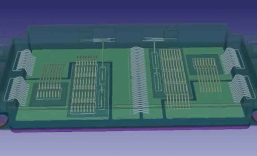
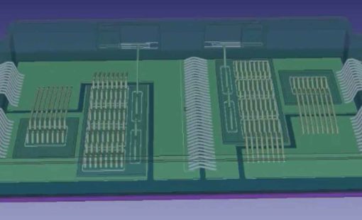
At EMPC 2019 visitors will have the opportunity to see how PCB designers can benefit from an early prototype input of chip and package data from the library as well as through the reuse of data from IC layout tools. The advanced PCB design capabilities of Zuken’s enterprise-level electronic design environment CR-8000 Design Force can be extended with powerful functionality for the design of single and multi-die packages for wire-bond, flip-chip, and high-density advanced packaging. Parametric wizards are available to guide users through the design process and streamline the creation of the system.
Read more about Zuken’s Advanced Packaging SolutionsAdvanced IC Packaging and Chip/Package/Board Co Design Environment
Lecturer: Iyad Rayane – Zuken Application Engineer
Sept 16th – 09:00 – 13:30
You should participate in this course if you are an IC package designer and chip physical implementation engineer working on the top-level implementation and the RDL routing in case of Flip Chip or Wafer Level packaging techniques. In his presentation, will outline a Co-Design flow for PCB and Advanced Packaging, providing practical examples of Advanced Packaging solution using Zuken’s CR-8000 tools:
- New design methodology for SiP
- Support for wizards and parametric creation of IC’s, BGA package, and 3D wire-bond placement
- Seamless connection of stacking IC’s and package on package (PoP)
- Package-specific design rules with real-time 3D checks and view
- Flip Chip I/O bump optimization
- I/O ring synthesis capability guarantees package routability
- “Tile-based” die bump placement and optimization
- Tape-out quality automatic routing for chip RDL and package escape routing
Contact
If you have any questions, please contact the Zuken event manager Francesca Libe. Email: francesca.libe@it.zuken.com
- Press Release
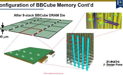
Zuken helps to overcome design challenges associated with 3D integration in the pursuit of next-generation semiconductor technologies.
- Webinar
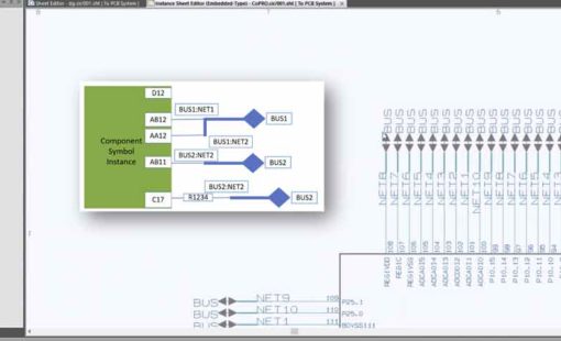
This webinar introduces a solution that automatically updates the pin assignments of ICs and complex connectors in PCB designs by reading pinout lists of SoC modules and multi-pin connectors into CR-8000 Design Gateway and automatically creates all required connections, buses, and hierarchy links in the schematic.
- Webinar
The typical design flow for a power module is in MCAD, where only structural analysis is possible. Moving to a new design flow using CR-8000 Design Force also allows for electrical analysis too. This webinar will demonstrate the features and benefits of this new design flow.