Tech Tip: Using Design Force Rule Editor to Calculate Track Impedance
Menu
Today are going to discuss how to use Design Force rule editor to calculate track impedance.
Calculate the track width value from the characteristic impedance and layer configuration by using a field solver.
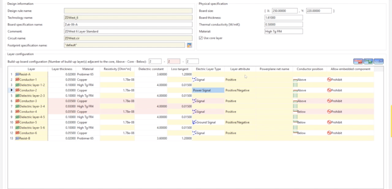
In [Layer Configuration] on the [Board Configuration] tab, set the thickness, resistivity, dielectric constant, and loss tangent values for all the layers.
Also, set the reference plane layer that matches the following conditions
A layer with the Layer attribute set to Power Plane is handled as a reference layer. If there is no Power Plane layer, a layer with the Electric layer type set to Power or Ground is handled as a reference plane. (The electric layer type of power or ground must be set for two or more layers.)
If the layer to be calculated is a power or ground layer, the power or ground layer located closest (upward or downward) to that layer is handled as a reference layer.
Click the [Calculate Char. Z -> Track Width] button in the upper part of the [Track width stack] table to open the dialog.
From the track width stack list, select the track width stack.
Set [Target Char. Z].
Set the [Rounding precision for track width] value
Calculate the track width value using a field solver until the specified rounding precision is reached.
Click the [Calculate Track Width] button. The calculation result is displayed in the [Track width] cell.
The range of track width that can be calculated is between 0.00001 mm and 5 mm.
Click the [Apply calculated results to track width stack] button to apply the track width value obtained from the calculation to the track width rule stack.
Differential Pairs are handled a little differently.
Click the [Calculate Diff. Z -> Track Width] button in the upper part of the [Differential pair rule stack] table to open the dialog.
From the track width stack list, select the differential pair rule stack.
Select [Calculation mode].
- Calculating track width from differential Z and track spacing
- Select [Track width] from [Calculation mode], and specify [Target Diff. Z] and [Track spacing].
- Calculating track spacing from differential Z and track width
- Select [Track spacing] from [Calculation mode] and specify [Target Diff. Z] and [Track width].
Set the [Rounding precision for track width (spacing)] value
Calculate the track width and spacing values using a field solver until the specified rounding precision is reached.
Click the [Calculate Track Width (Spacing)] button. The calculation result is displayed in the target cell (track width or spacing).
The range of track width and spacing that can be calculated is between 0.00001 mm and 5 mm.
Click the [Apply calculated results to diff. rule stack] button to apply the track width and spacing values obtained from the calculation to the differential pair rule stack.

-
Applications Engineer
Brian Gilman is an applications angineer, supporting customers with CR-8000/CR-5000 training and consulting. He works directly with the customers on a daily basis helping them work through the technical challenges they face. He loves to ski and must be on the first chairlift in the morning to lay down the first tracks on fresh powder.

- Webinar
April 12, 2024
Dealing with Component Obsolescence in PCB Design
This webinar will demonstrate how Zuken's CR-8000 Enterprise PCB Design System automates updates and redesigns in response to component obsolescence. Learn how to identify affected modules, update designs with a schematic module library, and intelligently assist layout modifications.
REGISTER
Live Webinar on June 11, 11 am CEST
- Webinar
July 12, 2022
Analysis and constraint-driven PCB Design with CR-8000 using analysis of SerDes
Using the example of the analysis of SerDes transmission paths such as PCI Express, SATA or USB3, we explain the methodology of an analysis- and constraint-driven assembly development with CR-8000 Design Force.
Watch Now

- Webinar
July 11, 2022
Electro Mechanical Design for Electronic Engineers: ECAD-MCAD Collaboration with CR-8000
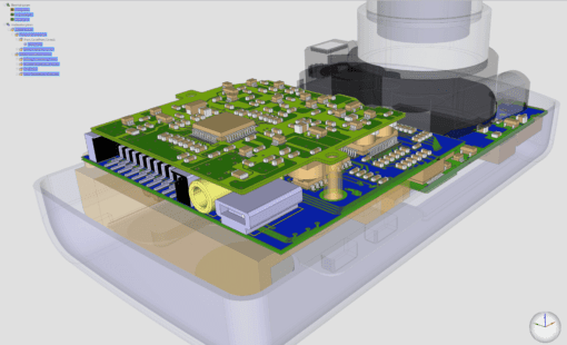
With its support of 3D, CR-8000 Design Force offers the possibility of validating PCB designs against the mechanical envelope. In this session you will learn how to use formats such as IDX and JT in Design Force or, alternatively, how to import native 3D data from various MCAD systems.
Watch Now

- Blog
December 13, 2021
High Speed Design Demystified: LPDDR4 Design Explained
A trend towards low power design prevails in the electronics industry today and is not likely to change in the near future. This development is driven by many reasons but primarily by the performance and storage density demands of mobile devices, where a reduction of the power consumption is crucial to extending battery life without sacrificing the bandwidth. This comprehensive guide helps you mitigate LPDDR4 Design.
Read now