Tech Tip: Routing a PCB design in a native 3D Tool
Menu
 PCB design tools were built on 2D software methods in the 1980s. Many of today’s design tools still use that 2D code base. Mechanical tools have moved on to native 3D design. PCB has been stuck more or less in the 2D world. Extensions to the 2D code base made 2.5D and 3D visualization possible. But designing in 3D requires the tool to be built on a 3D kernel.
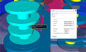
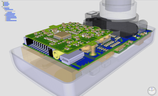
3D visualization of a PCB is essentially available in every PCB design tool on the market. However, 3D visualization is not a 3D design. Placing components on a PCB in a 3D view using accurate shape 3D models is 3D design. Another aspect of a 3D design is design rule checks for both collision and clearance utilizing 3D models of the components and the PC board enclosure. 3D design requires a 3D kernel that replaces the 2D modeling code base. Let’s get back to the purpose of this blog – native 3D routing.
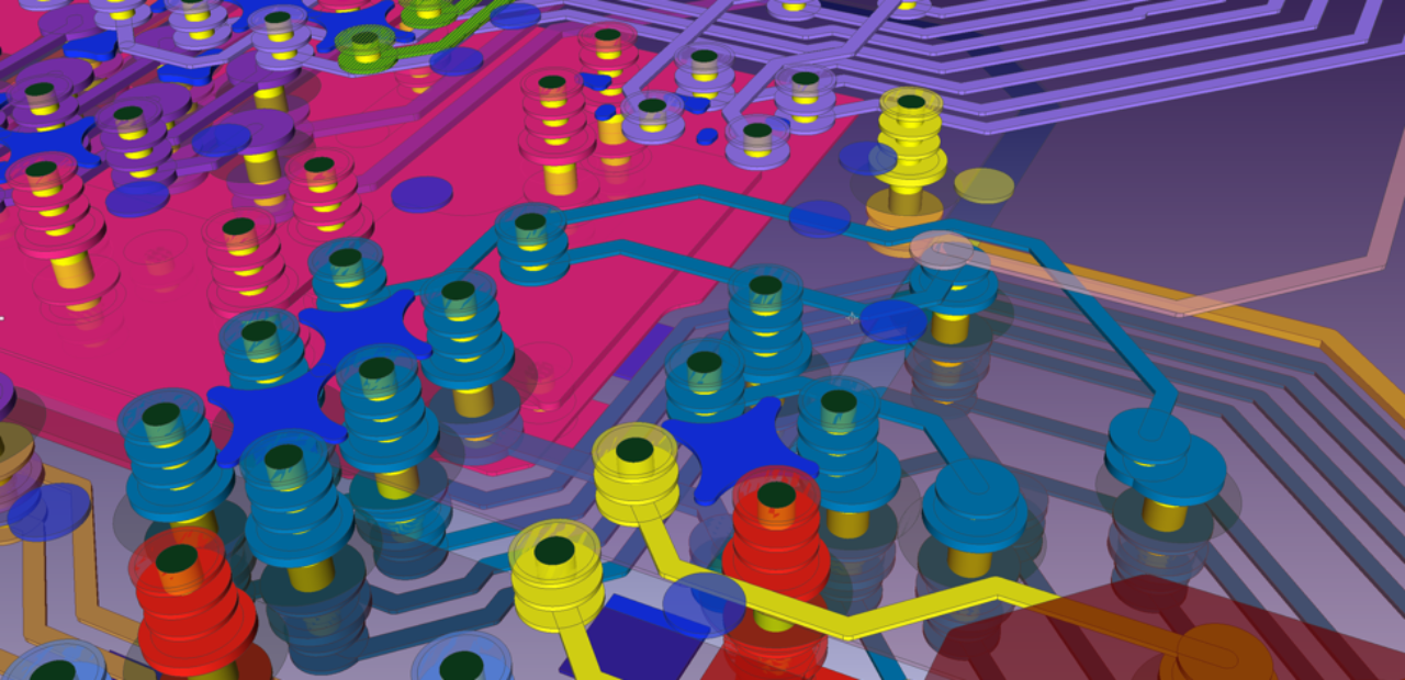
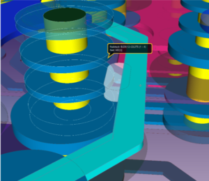
Have you tried it? The ability to fan-out micro vias under extremely small BGA footprints is difficult enough in a 2D topside view. The overlay of graphics primitives of filled lines and circles can be quite frustrating.
There are those tools that allow designers to quickly toggle from 2D routing to 3D views for a quick visualization only to have toggle back and forth to make the small adjustments to get the via placement just right.
What if you could route in 3D? Since the introduction of Zuken’s CR-8000 Design Force, users have been able to realize native 3D placement and routing. In fact, when we asked Design Force users how much time they spend actually routing in 3D versus 2D, the average response came back at approximately 45%. 2D design is very different from 3D and involves change. Not every PCB designer has decided to dive into 3D design mode.
Let’s take a look at some of the benefits of 3D routing that might change your mind.
- Real-time Visualization with transparency

- Less cycle picking to select the desired item.
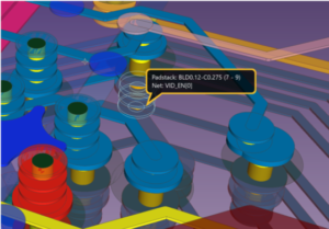
- Immediate DRC response.
- Take actions in 3D like trimming pads on specific layers
With Powerful 64 bit graphics equaling those used in modern gaming technologies PCB Designers can grow and become more efficient in their day to day placement and routing challenges.
If you have not experienced true 3D placement and routing, you should. You have to give it a try!

-
Technical Account Manager - Senior Applications Engineer
Andy Buja supports many disciplines of the Zuken Solutions family. In addition to providing both post and presales support to Zuken Customers and Partners, he focuses on crafting Zuken Solutions to meet emerging technology requirements. Mr. Buja has been a member of the Zuken team and its predecessors since 1985.
- Webinar
April 12, 2024
Dealing with Component Obsolescence in PCB Design
This webinar will demonstrate how Zuken's CR-8000 Enterprise PCB Design System automates updates and redesigns in response to component obsolescence. Learn how to identify affected modules, update designs with a schematic module library, and intelligently assist layout modifications.
REGISTER
Live Webinar on June 11, 11 am CEST

- Blog
January 11, 2024
Harnessing the power of artificial intelligence for PCB design
With the release of ChatGPT, artificial intelligence, has become a topic that has stirred many emotions. On our blog we're exploring whether AI could one day be used to support Zuken's core business of solving complex design challenges such as PCB layout and routing.
Read now
- Blog
December 04, 2023
DDR4 Design Masterclass: Advanced Techniques for Optimal Memory System Design
Although memory technology continues to evolve, in the current technology landscape, DDR4 is often a critical hurdle in the design process of an electronic application because of the large number of rules and constraints which have to be obeyed for the implementation of high-performance memory subsystems. Learn what to consider.
Read now

- Webinar
December 04, 2023
AI-Based PCB Place and Route
CR-8000 Webinar: Zuken recently announced the upcoming release of the industry’s first AI-based PCB place and route product - Autonomous Intelligent Place and Route (AIPR) - This webinar will examine how companies and users will benefit.
Watch Now
Related Content
- Products
October 01, 2018
Design Force
CR-8000 Design Force is the fastest, most effective PCB design solution available today. Design Force enables design teams to layout and verify their designs in the context of a complete system or product.
Read now
3D Multi-board PCB Design

- Products
September 26, 2018
CR-8000
CR-8000 is a System-Level PCB & IC Package Design software including 3D Multi-board, Analysis and MCAD Integration
Read now
Advanced multi-board PCB design software