Multi-board PCB Design for Applications With Different Voltages
Menu
The Benefits of Developing Multi-Layer PCB Designs
Stacking PCBs, as opposed to connecting with cables, in multi-board PCB design is a current and highly popular trend, as manufacturing costs are reduced and reliability improved. Herbert Ritthaler, Solution Architect Electronic Design, explains the benefits of developing the boards concurrently on a single CAD canvas.
At a glance
- Advanced applications such as electromobility require specialized functionality to be combined into a connected multi-board system.
- Whilst modules containing PCBs with dedicated functions have been around for decades, all e-mobility sectors are now looking at how the boards are physically connected.
- The advantages of board-stacking are many and most benefits derive from no longer needing mechanical connectors and cables. However, these benefits come at a price: The design process is now more complex.
- This article describes how Zuken’s CR-8000 Design Force supports such concurrent design in a single canvas.
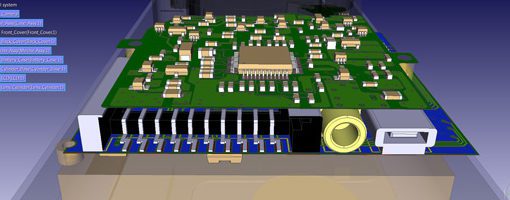
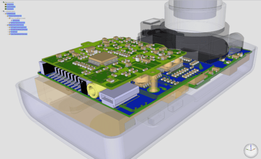
A multi-layer PCB design comprises two or more interconnected PCBs in a single enclosure. Typically, the boards will have very different roles. For example, if you consider e-mobility (i.e. the industry trend of switching over to electric drive trains and actuation in the automotive, aerospace and other transportation sectors), many modules are multi-board systems. One board will be a controller. Another will be for switching in and out potentially high current loads.
Whilst they will share many common design and manufacturing considerations, the PCBs will warrant special attention when it comes to their specific roles. In this respect, the controller board might be very high density, feature BGA devices (with hundreds of balls each), flip-chip devices, wire-bonded die, and/or have embedded components; i.e. the PCB substrate contains structures with resistive and/or capacitive properties.
The controller board may also feature high-speed digital and possibly even RF signals and assuring signal integrity through impedance matching will be of paramount importance. As for the power board, it may need to handle hundreds of Amps so thermal management may be the biggest challenge.
All in one
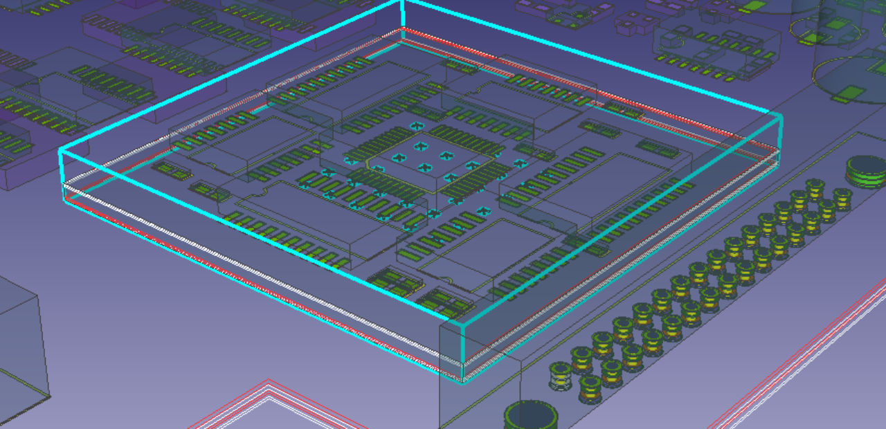
Modules containing PCBs with dedicated functions have been around for decades. However, all e-mobility sectors are now looking at how the boards are physically connected. A current trend is for them to be mounted one on top of the other. With the controller board placed as if it were a large BGA device on the power board.

The advantages of board-stacking are many and most benefits derive from no longer needing mechanical connectors and cables. For example, there are cost savings because there are fewer parts, assembly is simplified (also a cost-saving) and reliability is improved through virtue of not having the ‘mechanical’ links formed using connectors and cables.
However, these benefits come at a price. The design process is now more complex, and we are, for all intents and purposes, designing two PCBs at the same time. At least first-time around, after which one or both boards might be used in subsequent projects.
Clearly, the physical connections – i.e. where the module’s bumps will connect with solder-pasted pads on the main board – must align precisely and be electrically correct, i.e. there should be no signal mismatches between the boards.
Designing the boards – again, there might be two or more – in a single environment has considerable advantages. Zuken’s CR-8000 Design Force, for example, supports such concurrent design in a single canvas. At the schematic level, connector symbols are used to represent interfaces between the boards. These connectors initially exist as a temporary component on each board and build up the connectivity between both.
Multi-board PCB Design with Design Force
For layout purposes, it would be best to start with the controller board. Having defined its shape and size, all standard components would be placed. Most would be placed on the top side but, as mentioned, embedding (if only partially) is an option. Design Force automatically creates a temporary component for placement on the underside of the controller board. This temporary component exists initially as the connection point crosses as an indication of pad (or ball, if you prefer to think BGA) positions and padstacks.

Regarding the placement of each of the pads, the signals ‘intent’ must be a factor. In other words, for a signal that must connect with the base board, whilst routing from the pad of a topside component to the nearest pad on the underside might be practical for the controller board it may not be as convenient for base board to receive the signal from that physical location.
Next, the base board would be assigned a shape and dimensions. Again, all standard components would be placed. The controller board would be assigned to the temporary component of the base board schematic and subsequently placed at its intended position.

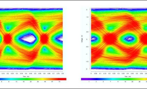
As with the assigning of signals to pads on the controller board, the same considerations apply for the base board. Signal integrity must be maintained through, for example, impedance matching for high-speed signals. Here, the beauty of working in a single canvas in Design Force is that impedance matching can be managed for signals that transition between boards.
Indeed, Design Force has several design rule-checks (DRCs) that will flag an infringement, such as failing to maintain a suitable galvanic isolation distance when routing high current signals. Accordingly, if the pad of one board is reassigned then executing an ‘update’ will keep the two design parts in sync. For example, to reduce crosstalk it is sometimes necessary to switch the +ve and -ve halves of an LVDS signal over. If the signal transitions boards, the inversion needs to be made on both.
Electrical updates are not the only ones that can be easily implemented. Sometimes, it will be necessary to move one or more pads relative to the others. And we have this flexibility as the underside of the controller board and its position on the base board exist as temporary components. The traditional BGA grid is a default starting pattern.
Multi-board PCB Designs Stacked in Your Favour
The benefits of designing the PCBs – at the schematic entry and board layout levels – for a multi-board module are considerable, and the practice is proving increasingly popular. Whether you regard the top board as a ‘component’ or as part of the single board (that happens to have different design requirements and therefore rules) is academic, and electrical and physical continuity (pads) is assured throughout.
Also, it does not matter if the board technologies vary considerably. For example, if the base board of a module is to be close to a heat source – such as a combustion engine or power inverter – then it can be prototyped in FR4, be functionally verified on the bench, then the design re-spun for ceramic. The controller board would then be a forced-air-cooled component on that board.
For more information on multi-board design in CR-8000 Design Force click here or download the whitepaper with the link below!
Download the full article as a PDF
You may also be interested in our on-demand webinar on 3D Multi-board PCB Design Basics. This webinar will discuss and demonstrate the key concepts behind a 3D multi-discipline design where supply chain, PCB, MCAD and analysis all converge into a next-generation design process.
Also see:

Richard Warrilow is a Technical Author with Declaration Limited. He is a qualified electronics engineer and worked for GEC Marconi Avionics (now BAE SYSTEMS) during the 1990s on two high-profile fly-by-wire programmes before moving into technical journalism and, latterly, establishing Declaration in 2001. Richard still works closely with companies active in the aerospace sector and has written articles on subject matters ranging from the certification of programmable electronic components intended for use in aerospace applications through to systems for the in-flight refuelling of military aircraft.
- Webinar
July 12, 2022
Analysis and constraint-driven PCB Design with CR-8000 using analysis of SerDes
Using the example of the analysis of SerDes transmission paths such as PCI Express, SATA or USB3, we explain the methodology of an analysis- and constraint-driven assembly development with CR-8000 Design Force.
Watch Now

- Webinar
July 11, 2022
Electro Mechanical Design for Electronic Engineers: ECAD-MCAD Collaboration with CR-8000
With its support of 3D, CR-8000 Design Force offers the possibility of validating PCB designs against the mechanical envelope. In this session you will learn how to use formats such as IDX and JT in Design Force or, alternatively, how to import native 3D data from various MCAD systems.
Watch Now
- Blog
December 13, 2021
High Speed Design Demystified: LPDDR4 Design Explained
A trend towards low power design prevails in the electronics industry today and is not likely to change in the near future. This development is driven by many reasons but primarily by the performance and storage density demands of mobile devices, where a reduction of the power consumption is crucial to extending battery life without sacrificing the bandwidth. This comprehensive guide helps you mitigate LPDDR4 Design.
Read now

- Webinar
September 15, 2021
CR-8000 with the Ansys Electronic Desktop
This webinar will introduce the use of the Ansys Electronic Database (EDB) format to share information from CR-8000 Design Force to Ansys, the advantages beyond the former ANF-based interface, and how this can help users be more effective and productive.
Watch Now
Related Content
- Webinar
October 20, 2018
3D PCB Multi-board Design Basics - Don't Fall Behind
Webinar, Design Force
- Products
October 01, 2018
Design Force
CR-8000 Design Force is the fastest, most effective PCB design solution available today. Design Force enables design teams to layout and verify their designs in the context of a complete system or product.
Read now
3D Multi-board PCB Design