High-Speed Design Challenges of Maintaining PCB Signal Integrity
Menu
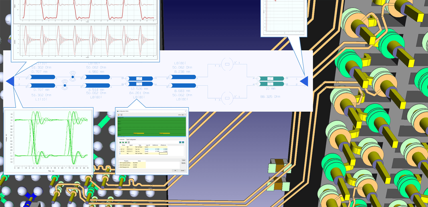
Ultra-high signal speeds demand detailed consideration of the third dimension in PCB design, including via structures and layer stacks. Today I’m going to focus on the challenge. In my two subsequent posts, I’ll be reviewing what PCB designers can do to meet that challenge.
Mainstream high-speed signals
Not long ago, third dimension issues didn’t figure too much in high-speed design calculations; but signals have become so fast that those vias don’t affect them the same way they did before. Those really fast signals have become part of super-common bus standards that are used in all kinds of products.
It’s a PCB design issue that we can’t avoid. Luckily, there are ways not just to address this issue, but to optimize performance at the same time.
Effects of vias on PCB signal integrity
Layer changes can slow signals down or distort them. Their effects depend (amongst other things) on:
- Via geometry
- Where vias are placed within the routing
- Shape and speed of signals
- Other nearby items that couple to vias
So vias don’t always distort signals in the same way and neither does the same via always introduce the same delay.
New via technology threshold
A key breakpoint is reached when a signal is so fast that the routing that carries it starts to behave as a network of transmission lines. When this happens, engineers must take positive steps to make sure signals arrive in good shape.
For mainstream digital designs, that breakpoint was reached decades ago for routing in the XY plane. That’s why we’ve long had controlled routing topology and reference ground and power planes. But now we’ve reached the point where we need to do the same in the third dimension. Standards-based bussing means that this can happen even on a board that doesn’t run particularly quickly.
If you’d like to see me describe all that with the help of a sheet of hardboard, you can watch this short movie.
See you again in Part 2 where I look more at how to use vias to maintain PCB signal integrity under these high-speed 3D conditions.
-
Electronic Design Technology Partner
Jane Berrie is an EDA product innovator and technical marketing content creator, focusing on high-speed design and signal integrity. She is a published author of technical articles and a past session chair at the annual Design Automation Conference (DAC). Jane enjoys managing themed charity events, disco and going out with friends.
- Webinar
April 12, 2024
Dealing with Component Obsolescence in PCB Design
This webinar will demonstrate how Zuken's CR-8000 Enterprise PCB Design System automates updates and redesigns in response to component obsolescence. Learn how to identify affected modules, update designs with a schematic module library, and intelligently assist layout modifications.
REGISTER
Live Webinar on June 11, 11 am CEST

- Blog
January 11, 2024
Harnessing the power of artificial intelligence for PCB design
With the release of ChatGPT, artificial intelligence, has become a topic that has stirred many emotions. On our blog we're exploring whether AI could one day be used to support Zuken's core business of solving complex design challenges such as PCB layout and routing.
Read now
- Blog
December 04, 2023
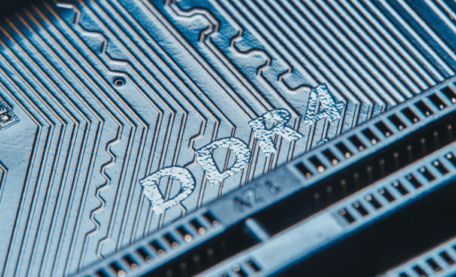
DDR4 Design Masterclass: Advanced Techniques for Optimal Memory System Design
Although memory technology continues to evolve, in the current technology landscape, DDR4 is often a critical hurdle in the design process of an electronic application because of the large number of rules and constraints which have to be obeyed for the implementation of high-performance memory subsystems. Learn what to consider.
Read now

- Webinar
December 04, 2023
AI-Based PCB Place and Route
CR-8000 Webinar: Zuken recently announced the upcoming release of the industry’s first AI-based PCB place and route product - Autonomous Intelligent Place and Route (AIPR) - This webinar will examine how companies and users will benefit.
Watch Now
