Defining and Routing PCB Constraints for DDR3 Memory Circuits: How-to Movies
Menu
As Zuken technology partners, we are often asked about how best to set PCB constraints for double-data-rate (DDR) memory, and how to route to those constraints. This question arose recently when we were asked to create a common style of DDR3 design for training, and we tried mining the web for detailed information on PCB constraints. There had to be something out there, we thought.
We were right; but unfortunately the detail had to be excavated from a vast and comprehensive pile of information about devices and controllers. It was hard to find a brief but clear description of what a PCB designer needs, and why, for a basic DDR3 circuit.
PCB Design of a DDR3 Memory Circuit
Necessity being the mother of invention I worked with Kevan Keech, an expert PCB designer, to create the most straightforward, realistic example we could think of – captured in three short movies.
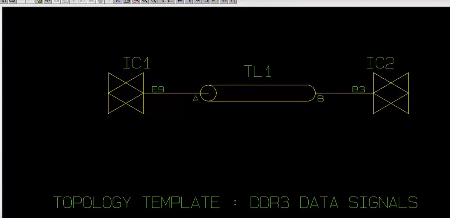
In the first movie I explain the circuit, routing topology and constraints.
In the second movie, Kevan constrains the PCB design.
In the final movie, Kevan routes the PCB design step-by-step and at the end we summarize the results.
We use a single design example from start to finish – a controller connected to five 1-Gbitx8 SDRAM devices. Levelling is enabled so that the SDRAMs can be routed using fly-by topology, as defined in JEDEC standards and elsewhere.
After watching these movies, you will understand:
- What key routing constraints you need for a memory circuit, such as that outlined in the movies
- How to adjust routing to balance impedance of lead-in and loaded sections as specified in JEDEC standards and why you might need to do so
- How to place SDRAM components for optimum performance
- How to constrain the PCB design
- How to route accurately to DDR3 constraints
- How to ensure constraints have been met.
We hope you enjoy the movies and find them useful.
If you’ve taken a look, why not leave a comment below!
This blog post was co-written by John Berrie and Kevan Keech, based in the Zuken, Bristol, UK office.

-
Electronic Design Technology Partner
Jane Berrie is an EDA product innovator and technical marketing content creator, focusing on high-speed design and signal integrity. She is a published author of technical articles and a past session chair at the annual Design Automation Conference (DAC). Jane enjoys managing themed charity events, disco and going out with friends.

- Webinar
April 12, 2024
Dealing with Component Obsolescence in PCB Design
This webinar will demonstrate how Zuken's CR-8000 Enterprise PCB Design System automates updates and redesigns in response to component obsolescence. Learn how to identify affected modules, update designs with a schematic module library, and intelligently assist layout modifications.
REGISTER
Live Webinar on June 11, 11 am CEST

- Blog
January 11, 2024
Harnessing the power of artificial intelligence for PCB design
With the release of ChatGPT, artificial intelligence, has become a topic that has stirred many emotions. On our blog we're exploring whether AI could one day be used to support Zuken's core business of solving complex design challenges such as PCB layout and routing.
Read now
- Blog
December 04, 2023
DDR4 Design Masterclass: Advanced Techniques for Optimal Memory System Design
Although memory technology continues to evolve, in the current technology landscape, DDR4 is often a critical hurdle in the design process of an electronic application because of the large number of rules and constraints which have to be obeyed for the implementation of high-performance memory subsystems. Learn what to consider.
Read now

- Webinar
December 04, 2023
AI-Based PCB Place and Route
CR-8000 Webinar: Zuken recently announced the upcoming release of the industry’s first AI-based PCB place and route product - Autonomous Intelligent Place and Route (AIPR) - This webinar will examine how companies and users will benefit.
Watch Now
