CR-8000 Design Force

- Blog
Januar 25, 2023
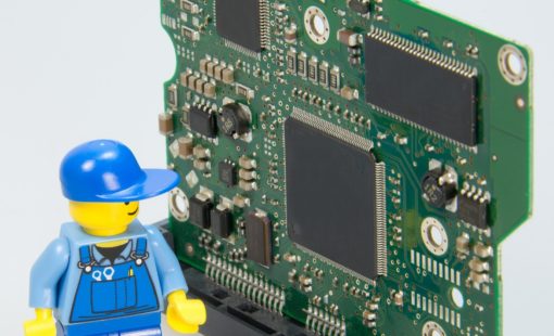
PCB constraints should drive your design flow. Here’s why.
We've all heard of PCB design constraints. They're those little things that limit our ability to create the perfect board in very short periods of time. But what exactly are they? And why do they matter? This blog post elaborates on PCB constraints and why they should drive your design flow.
Read now

- Blog
November 28, 2022
Boosting Power-Integrity-Analysis Performance by Introducing a Multi-Threading-Simulation Architecture
Zuken is taking its Simulation and Analysis Performance to the next level by introducing a new processing technology to its PI/EMI analysis tool. Multi-threading will speed up PI analysis which will give PCB designers a boost in productivity, especially when evaluating different design alternatives for PDN structures.
Read now

- Blog
Dezember 13, 2021
LPDDR4 Design für PCB Entwickler
In der Elektronikindustrie herrscht heute ein anhaltender Trend zum Low-Power-Design und das wird sich wohl auch in näherer Zukunft kaum ändern. Angetrieben wird er unter anderem von den Anforderungen und Leistung und Speicherdichte von mobilen Geräten, bei denen eine Reduzierung des Stromverbrauchs entscheidend ist, um die Akkulaufzeit zu verlängern, ohne dabei die Bandbreite zu beeinträchtigen. Dieser Guide hilft Ihnen, die Herausforderungen von LPDDR4-Design zu lösen.
Read now

- Blog
Juni 03, 2021
Ist das 3D Elektronik Design auf der Höhe der Zeit?
Viele Jahre lang war das Layout einer Leiterplatte in 2D für die meisten Mainstream-Technologien ausreichend. Heute stehen Produktentwickler im Elektronikbereich jedoch vor neuen Herausforderungen, ausgelöst durch Megatrends wie beispielsweise das Internet of Things. Können die heutigen CAD-Tools also die neuen Anforderungen erfüllen und die Vorteile der neuen Technologien ausschöpfen?
Read now

- Blog
Mai 17, 2021
Back-Drilling Vias: Kosten sparen und Übersprechen verhindern
Back-Drilling, das nachträgliche Ausbohren von nicht benötigten Durchkontaktierungen, ist eine kostengünstige Alternative zu Blind und Buried Durchkontaktierungen in der Multilayer-Leiterplattenfertigung.
Read now
- Blog
April 15, 2021
Tech Tip: 3D Kollisions- und Abstandsprüfungen im Multi-Board Design
Die Überprüfung auf potenzielle elektromechanische Kollisionen wird normalerweise eher im mechanischen Umfeld durchgeführt. Die Verlagerung der Prüfung in den elektrischen Bereich während der Komponentenplatzierung kann jedoch dazu beitragen, ein zuverlässigeres Produkt zu entwickeln. In Design Force gibt es integrierte Checks, die den Entwurf auf Kollisionen und Abstandsvorgaben prüfen.
Read now
- Blog
September 24, 2020
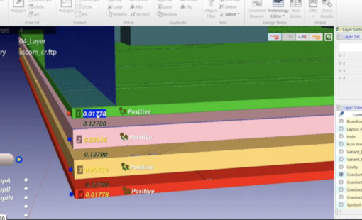
Tech Tip: Design Force 3D Technology Editor
In Design Force you can edit your board Technology using the 3D Technology Editor. In the 3D technology edit window, you can perform the following operations to edit the technology for the board.
Read now
- Blog
September 10, 2020
Leistungsstarke SI/PI/EMV PCB-Simulationssoftware verkürzt die Analysezeit um 86%
Was tun, wenn Ihr nächstes Projekt besonders hohe EMV-Anforderungen stellt und schneller als jemals zuvor abgeschlossen werden muss?
Read now
- Blog
August 25, 2020
Tech-Tip: Checking Data Outside the Board
Board design rule checks only check up to the board outline. If you had dropped or moved some data outside the board outline there was no check for this until now...
Read now
- Blog
August 20, 2020
Exploring What’s New in CR-8000 2020
What drives the features that are added or updated in a new release? The majority of the changes or additions in any Zuken tool release are customer-driven. Our customers provide valuable insight into emerging technologies, process and methodology changes, and the direction in which their EDA needs are taking them. This post focuses on the high points of the CR-8000 2020 release.
Read now
- Blog
Juli 07, 2020
Tech-Tip: Creating a Connector Pin Netlist
Checking the pinout of your connectors is an important part of creating your printed circuit board. Checking your pin connections can save you from a costly re-spin of your circuit board. This can be done using the Constraint Browser in Design Force. By default, the Constraint Browser does not show this information.
Read now
- Blog
März 26, 2020
Multi-Board-Design für Anwendungen mit unterschiedlichen Spannungen
Die Vorteile der Entwicklung aller Platinen eines Multi-Board Systems in einem durchgängigen System. Das so genannte Stacking von Platinen -das Stapeln von Leiterplatten als Alternative zur Verbindung über Kabeln - ist ein aktueller Trend, der die Herstellungskosten senken und die Zuverlässigkeit verbessern kann.
Read now
- Blog
Januar 21, 2020
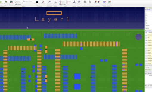
Tech Tip: Design Force Cut Land
When design space is at a premium, sometimes traces can be at risk of being exposed by any misregistration of the solder mask. If you have this situation use the “Cut Land” option under the Track tab in Design Force.
Read now
- Blog
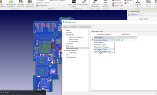
November 19, 2019
Tech Tip: How to export MCAD data from CR-8000 Design Force to enable faster thermal simulation in ANSYS Icepak
This video demonstrates how you can export a STEP file from CR-8000 Design Force including automatically editing your package shape and deformation spec to reduce heat transfer and fluid flow simulation time in ANSYS Icepak.
Read now

- Blog
September 19, 2019
Tech-Tip: Setting a temporary grid in Design Force
Offsetting your Grid can be very useful when your component pads do not fall on the current Grid.
Read now
- Blog
Juli 19, 2019
Tech Tip: How to Transfer ABL File From CR-8000 Design Force to Keysight ADS Momentum
This video illustrates how to import and export ABL file from CR-8000 Advanced PCB Design Software Design Force tool to Keysight Technology’s Advanced Design Systems (ADS) Momentum Tool.
Read now